
Products
Related Posts
What is
GA9354C
?

Category:


Single +3V power supply Low insertion loss: 0.5 dB @ 2000 MHz
|
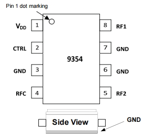
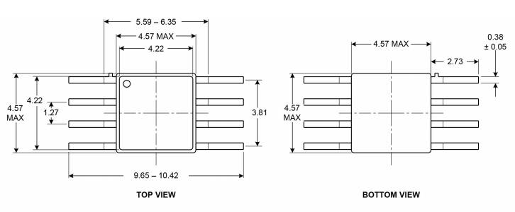
Pin Configuration
|
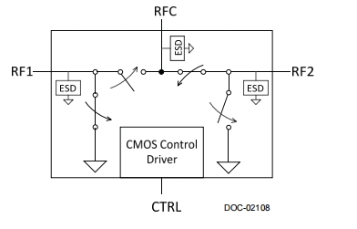
Functional Diagram
|
 |
 |
|
Parameter
|
Condition
|
Min
|
Typ
|
Max
|
Unit
|
|
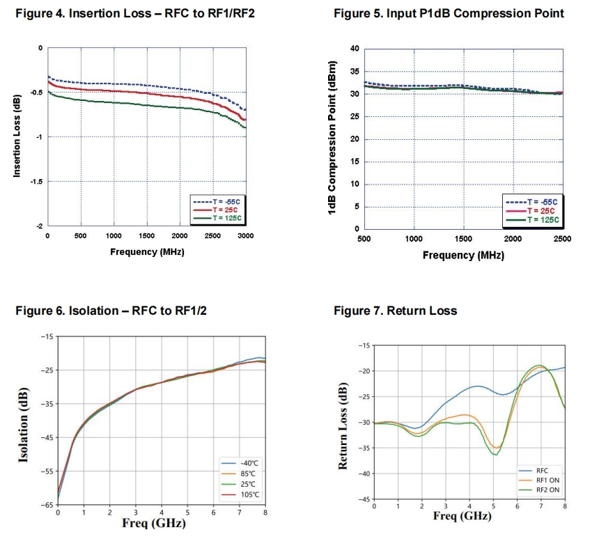
Operation frequency 2 DC 6000
|
DC
|
6000
|
MHz
|
||
|
Insertion loss
|
2000 MHz
|
0.5
|
0.70
|
dB
|
|
|
Isolation – RFC to RF1/RF2
|
2000 MHz
|
40
|
45
|
dB
|
|
|
Isolation – RF1 to RF2
|
2000 MHz
|
32
|
35
|
dB
|
|
|
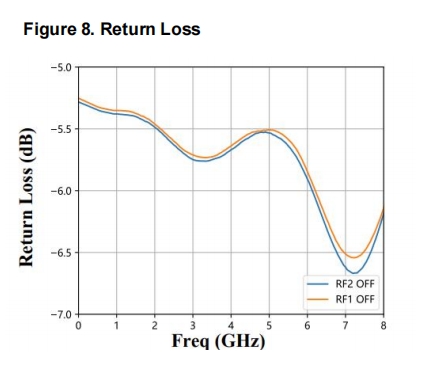
Return loss3
|
2000 MHz
|
20
|
dB
|
||
|
Input P1dB compression point
|
2000 MHz
|
28
|
30
|
dBm
|
|
Table 2. Pin Descriptions
|
Table 3. DC Electrical Specifications
|
|||||||
|
Pin #
|
Pin Name
|
Description
|
Parameter
|
Min
|
Typ
|
Max
|
Unit
|
|
| 1 |
VDD
|
Nominal +3V supply connection
|
Supply voltage, VDD
|
2.7
|
3.0
|
3.6
|
V
|
|
| 2 |
CTRL
|
CMOS or TTL logic level:
High = RFC to RF1 signal path.
Low = RFC to RF2 signal path.
|
Input leakage
|
–1
|
1
|
μA
|
||
| 3 |
GND
|
Ground connection. Traces should be
physically short and connected to ground
plane for best performance.
|
Supply current, IDD (VDD = 3V, VCTRL = 3V) |
μA
|
||||
| 4 |
RFC
|
Common RF port for switch.*
|
Control voltage high
|
V
|
||||
| 5 |
RF2
|
RF2 port.*
|
Control voltage low
|
V
|
||||
| 6 |
GND
|
Ground connection. Traces should be
physically short and connected to ground
plane for best performance.
|
Absolute maximum ratings are those values listed in the following table.
Exceeding these values maycause permanent device damage.
Functional operation should be restricted to the limits in the DC Electrical Specifications table. Exposure to absolute
maximum ratings for extended periods may affect device reliability.
|
|||||
| 7 |
GND
|
Ground connection. Traces should be
physically short and connected to ground
plane for best performance.
|
||||||
| 8 |
RF1
|
RF1 port.*
|
Table 4. Absolute Maximum Ratings
|
|||||
|
GND
|
GND
|
Bottom of the package is ground.
Connecting the bottom of the package to
ground is required
|
Symbol
|
Parameter/Condition
|
Min
|
Max
|
Unit
|
|
|
Electrostatic Discharge (ESD) Precautions When handling this UltraCMOS device, observe the same precautions that you would use with other ESD-sensitive devices. Although this device contains circuitry to protect it from damage due to ESD, precautions should be taken to avoid exceeding the rating specified in Table 3. Latch-Up Immunity Unlike conventional CMOS devices, UltraCMOS devices are immune to latch-up. |
VDD
|
Power supply voltage
|
–0.3
|
5.0
|
V
|
|||
|
VI
|
Voltage on any input except for the CTRL input
|
V
|
||||||
|
VCTRL
|
Voltage on CTRL input
|
5.0
|
V
|
|||||
|
TST
|
Storage temperature range
|
–65
|
+150
|
°C
|
||||
|
Table 5. Control Logic Truth Table
|
TOP
|
Operating temperature range
|
–40
|
+105
|
°C
|
|||
|
Control Voltage
|
Signal Path
|
PIN
|
Input power (50Ω,CW)
|
35
|
dBm
|
|||
|
CTRL = CMOS or TTL High
|
RFC to RF2
|
ΘJC
|
Theta JC
|
57
|
°C/W
|
|||
|
CTRL = CMOS or TTL Low
|
RFC to RF1
|
Tj
|
Junction temperature
|
+125
|
°C
|
|||
|
The control logic input pin (CTRL) is typically driven by a +3V CMOS logic level signal, and has a threshold of 50% of VDD. For flexibility to support systems that have 5-volt control logic drivers, the control logic input has been designed to handle a 5-volt logic HIGH signal. (A minimal current will be sourced out of the VDD pin when the control logic input voltage level exceeds VDD.)
|
VESD
|
ESD voltage
(Human Body Model)
|
200
|
V
|
||||
|
TID
|
Total cumulative exposure to
ionizing radiation
|
100
|
kRad(Si)
|
|||||
Previous
Next
Inquire Now
Note: Please leave your email address, our professionals will contact you as soon as possible!
Related Products