Products

What is

GA5057VF

?

+
7.1-8.8GHz Power Amplifier MMIC FEATURES High Output Power: 33.0dBm(typ.) High Linear Gain: 30.0dB(typ.) Low VSWR Broad Band: 7.1~8.8GHz Impedance Matched Zin/Zout = 50Ω 
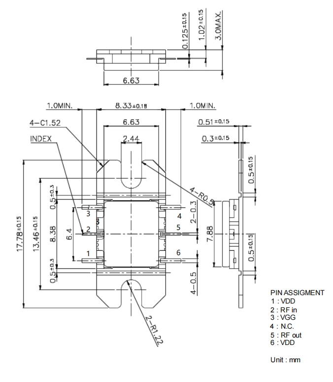
Small Hermetic Metal-Ceramic Package(VF)
div[class^="e_richText"] .table table.buyao td {border:none !important;}

Category:

DESCRIPTION
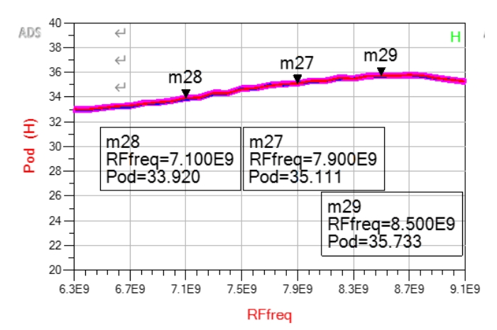
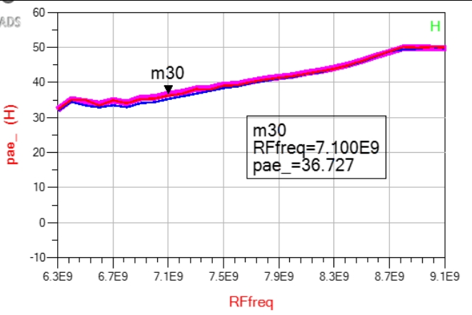
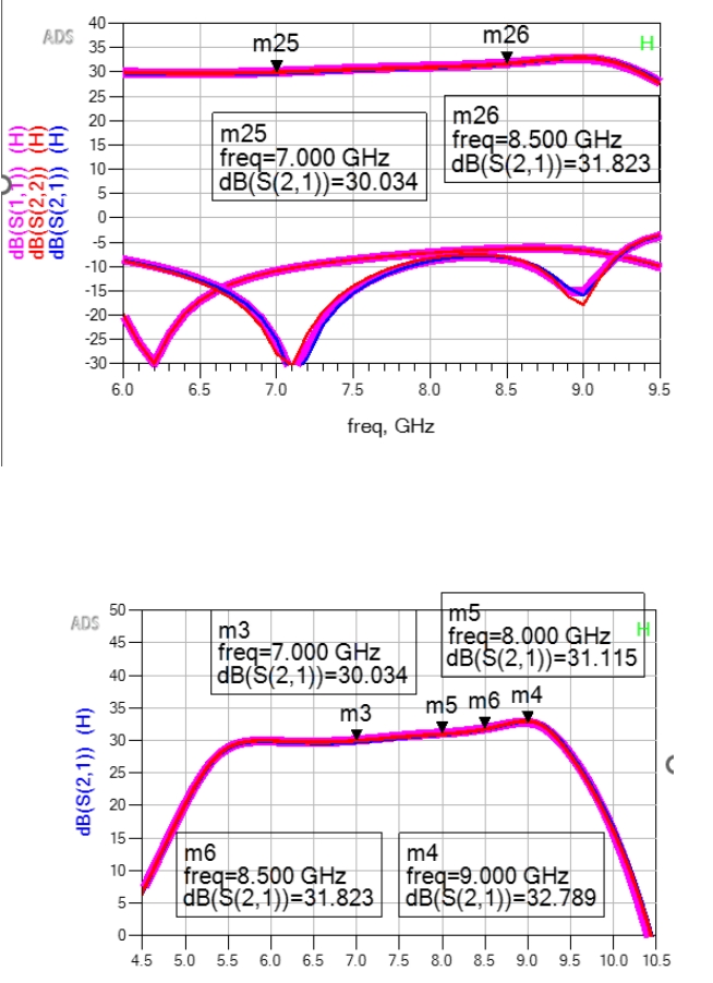
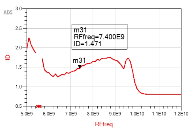
The GA5057VF is a MMIC amplifier that contains a four-stage amplifier, internally matched, for standard communicationsband in the 7.1 to 8.8GHz frequency range.
ABSOLUTE MAXIMUM RATINGS (Case Temperature Tc=2 )
Item
Symbol
Rating
Unit
DC Input Voltage
VDD
10
V
DC Input Voltage
VGG
-5
V
Input Power
Pin
14
dBm
Storage Temperature
Tstg
-55 to +125
Recommended Operating Condition
Item
Symbol
Condition
Unit
DC Input Voltage at Tc=25
VDD
10
V
Input Power at Tc=25
Pin
10
dBm
DC Input Current at Tc=25
IDD
1400
mA
Operating Case Temperature
Tc
-40 to +85
ELECTRICAL CHARACTERISTICS (Case Temperature Tc=2 )
Item
Symbol
Test Conditions
Limit
Unit
Min.
Typ.
Max.
Frequency Range
f
 
7.1 - 8.8
GHz
dBm
Output Power at 1dB G.C.P.
P1dB
 
VDD=10V
VGG=-5V
f=7.1 to 8.5GHz
32.0
34.0
-
Power Gain at 1dB G.C.P.
G1dB
23.0
26.0
-
dB
Gain Flatness
ΔG
-
2.4
4.0
dB
-
Input VSWR
VSWRi
-
2 : 1
2.6 : 1
Output VSWR
VSWRo
-
2 : 1
-
-
DC Input Current
IDD
VDD=10V,VGG=-5V
-
1100
1200
mA
DC Input Current
IGG
-
5.0
15.0
mA
Channel Temperature Rise
ΔTch
-
50
-


Inquire Now

Note: Please leave your email address, our professionals will contact you as soon as possible!

Related Products

GA9354C


The GA29F040 is a 4-mega bit Flash memory organized as 512K bytes of 8 bits. Flash memories offer the most cost-effective and reliable read/write non volatile random access memory. The GA29F040 is packaged in 32-pin PLCC, TSOP, PDIP. It is designed to be reprogrammed and erased in system or in standard EPROM programmers. The standard GA29F040 offers access time as fast as 55ns, allowing operation of high-speed microprocessors without wait states. To eliminate bus contention, the GA29F040 has separate chip enable (CE#) and output enable (OE#) controls. Flash memories augment EPROM functionality with incircuit electrical erasure and programming. The GA29F040 uses a command register to manage this functionality. The command register allows for 100% TTL level control inputs and fixed power supply levels during erase and programming, while maintaining maximum EPROM compatibility. Flash technology reliably stores memory con- tents even after 100,000 erase and program cycles. The cell is designed to optimize the erase and program mechanisms. In addition, the combi- nation of advanced tunnel oxide processing and low internal electric fields for erase and programming operations produces reliable cycling. The GA29F040 uses a 5.0V 10% VCC supply to per- form the High Reliability Erase and auto Program/ Erase algorithms. The highest degree of latch-up protection is achieved with proprietary non-epi process. Latch-up protection is proved for stresses up to 100 milliamps on address and data pin from -1V to VCC + 1V.

GA29F040


The GA29F040 is a 4-mega bit Flash memory organized as 512K bytes of 8 bits. Flash memories offer the most cost-effective and reliable read/write non volatile random access memory. The GA29F040 is packaged in 32-pin PLCC, TSOP, PDIP. It is designed to be reprogrammed and erased in system or in standard EPROM programmers. The standard GA29F040 offers access time as fast as 55ns, allowing operation of high-speed microprocessors without wait states. To eliminate bus contention, the GA29F040 has separate chip enable (CE#) and output enable (OE#) controls. Flash memories augment EPROM functionality with incircuit electrical erasure and programming. The GA29F040 uses a command register to manage this functionality. The command register allows for 100% TTL level control inputs and fixed power supply levels during erase and programming, while maintaining maximum EPROM compatibility. Flash technology reliably stores memory con- tents even after 100,000 erase and program cycles. The cell is designed to optimize the erase and program mechanisms. In addition, the combi- nation of advanced tunnel oxide processing and low internal electric fields for erase and programming operations produces reliable cycling. The GA29F040 uses a 5.0V 10% VCC supply to per- form the High Reliability Erase and auto Program/ Erase algorithms. The highest degree of latch-up protection is achieved with proprietary non-epi process. Latch-up protection is proved for stresses up to 100 milliamps on address and data pin from -1V to VCC + 1V.

Business license

Address: Beijing Tongzhou District Xiji Town, Wanganyuan Innovation Center 1-198