
Products
Related Posts
What is
GA29F040
?

The GA29F040 is a 4-mega bit Flash memory organized as 512K bytes of 8 bits. Flash memories offer the most cost-effective and reliable read/write non volatile random access memory. The GA29F040 is packaged in 32-pin PLCC, TSOP, PDIP. It is designed to be reprogrammed and erased in system or in standard EPROM programmers. The standard GA29F040 offers access time as fast as 55ns, allowing operation of high-speed microprocessors without wait states. To eliminate bus contention, the GA29F040 has separate chip enable (CE#) and output enable (OE#) controls.
Flash memories augment EPROM functionality with incircuit electrical erasure and programming. The GA29F040 uses a command register to manage this functionality. The command register allows for 100% TTL level control inputs and fixed power supply levels during erase and programming, while maintaining maximum EPROM compatibility. Flash technology reliably stores memory con- tents even after 100,000 erase and program cycles. The cell is designed to optimize the erase and program mechanisms. In addition, the combi- nation of advanced tunnel oxide processing and low internal electric fields for erase and programming operations produces reliable cycling. The GA29F040 uses a 5.0V 10% VCC supply to per- form the High Reliability Erase and auto Program/ Erase algorithms. The highest degree of latch-up protection is achieved with proprietary non-epi process. Latch-up protection is proved for stresses up to 100 milliamps on address and data pin from -1V to VCC + 1V.
div[class^="e_richText"] .table table.buyao td {border:none !important;}Category:


FEATURES
|
• 524,288 x 8 only
• Single power supply operation
- 5.0V only operation for read, erase and program operation
• Fast access time: 55/70/90ns
• Compatiblewith29F040device
• Low power consumption
- 30mA maximum active current(5MHz)
- 1uA typical standby current
• Command register architecture
- Byte Programming (9us typical)
- Sector Erase
8 equal sectors of 64K-Byte each
• Auto Erase (chip & sector) and Auto Program
- Automatically erase any combination of sectors with Erase Suspend capability
- Automatically program and verify data at specified address
• Erase suspend/Erase Resume
- Suspends an erase operation to read data from, or program datato,anothersectorthat is not beingerased,then resumes the erase
|
• Status Reply
- Data# Polling & Toggle bit for detection of program and erase cycle completion
• Sector protect/chip unprotect for 5V only system
• Sector protection
- Hardware method to disable any combination of sectors from program or erase operations
- Temporary sector unprotect allows code changes in previously locked sectors
• 100,000 minimum erase/programcycles
• 100,000 minimum erase/program cycles
• Latch-up protected to 100mA from -1V toVCC+1V
• Low VCC write inhibit is equal to or less than 3.2V
• Package type:
- 32-pin PLCC, TSOP or PDIP
- All Pb-free devices are RoHS Compliant
• Compatibility with JEDEC standard
- Pinout and software compatible with single-power supply Flash
• 20 years data retention
|
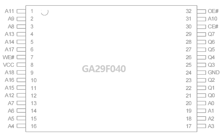
PIN CONFIGURATIONS
|
32 PDIP
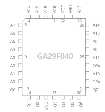 |
32 PLCC
|
|
32TSOP (StandardType) (8mm x 20mm)
 |
|
|
PIN DESCRIPTION
|
SECTOR STRUCTURE
|
||||||
|
SYMBOL
|
PIN NAME
|
29F040 SECTOR ADDRESS TABLE
|
|||||
|
A0~A18
|
Address Input
|
Sector
|
A18
|
A17
|
A16
|
Address Range
|
|
|
Q0~Q7
|
Data Input/Output
|
SA0
|
0
|
0
|
0
|
00000h-0FFFFh
|
|
|
CE#
|
Chip Enable Input
|
SA1
|
0
|
0
|
1
|
10000h-1FFFFh
|
|
|
WE#
|
Write Enable Input
|
SA2
|
0
|
1
|
0
|
20000h-2FFFFh
|
|
|
OE#
|
Output Enable Input
|
SA3
|
0
|
1
|
1
|
30000h-3FFFFh
|
|
|
GND
|
Ground Pin
|
SA4
|
1
|
0
|
0
|
40000h-4FFFFh
|
|
|
VCC
|
+5.0V single power supply
|
SA5
|
1
|
0
|
1
|
50000h-5FFFFh
|
|
|
SA6
|
1
|
1
|
0
|
60000h-6FFFFh
|
|||
|
SA7
|
1
|
1
|
1
|
70000h-7FFFFh
|
|||
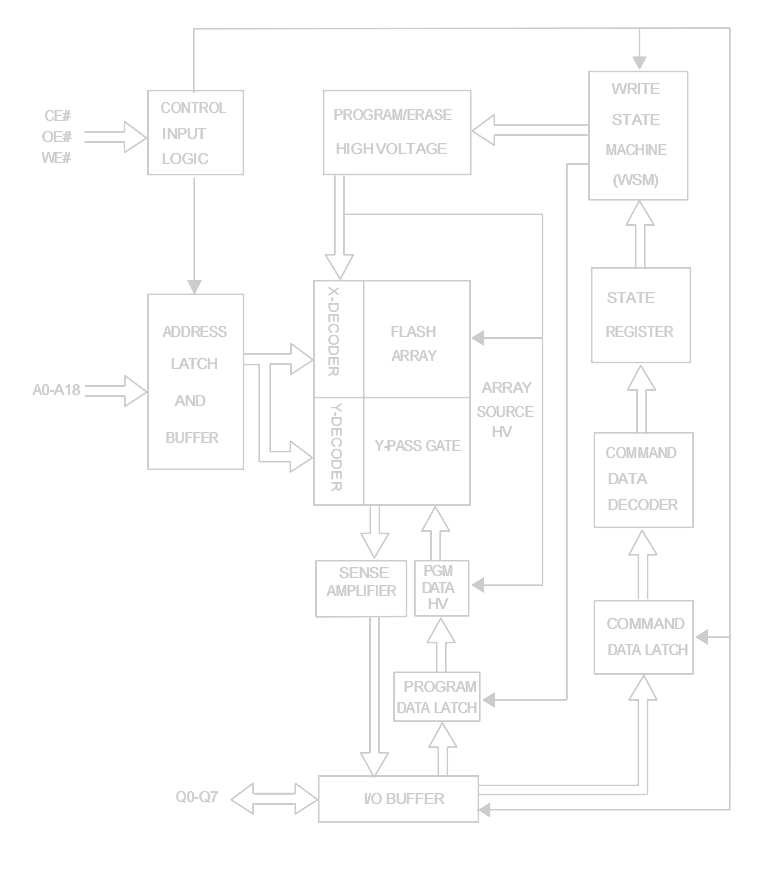
BLOCK DIAGRAM
|
AUTOMATIC PROGRAMMING
The 29F040 is byte programmable using the Auto matic Programming algorithm. The Automatic Program ming algorithm makes the external system do not need to have time out sequence nor to verify the data pro grammed. The typical chip programming time at room temperature of the 29F040 is less than 4.5 sec- onds.
|
AUTOMATIC ERASE ALGORITHM
Automatic Erase algorithm requires the user to write commands to the command register using stand- ard microprocessor write timings. The device will automatically pre-program and verify the entire array. Then the device automatically times the erase pulse width,provides the erase verification, and counts the number of sequences. A status bit toggling between consecutive read cycles provides feedback to the user as to the status of the programming operation.
Register contents serve as inputs to an internal statemachine which controls the erase and programming circuitry. During write cycles, the command register internally latches address and data needed for the programming and erase operations. During a system write cycle, addresses are latched on the falling edge of WE# or CE#, whichever happens later, and data are latched on
the rising edge of WE# or CE#, whichever happens first.
Flash technology combines years of EPROM experience to produce the highest levels of quality, reliability, and cost effectiveness. The 29F040 electri- cally erases all bits simultaneously using Fowler-Nord- heim tunneling. The bytes are programmed by using the EPROM programming mechanism of hot electron injection.
respond to any command set. cycle, program the a program command sequences cycle, register and the command will state During a Sector Erase only -machine respond register will to will control Erase not Suspend command. After Erase Suspend is completed, the device stays in read mode. After the state machine has completed its task, it will allow the command register to respond to its full command set.
|
|
AUTOMATIC CHIP ERASE
The entire chip is bulk erased using 10 ms erase pulses according to Automatic Chip Erase algorithm. Typical erasure at room temperature is accomplished in less than 4 second. The Automatic Erase algorithm automatically programs the entire array prior to electrical erase. The timing and verification of electrical erase are controlled internally within the device.
|
|
|
AUTOMATIC SECTOR ERASE
The Erase algorithm. the array to be erased in one erase cycle. Automatic Sector Erase algorithm auto programs the specified sector(s) prior to electrical 29F040 is sector(s) erasable using Sector erase modes allow sectors of Auto Sector - matically The erase. The timing and verification of electri- cal erase are controlled internally within the device.
|
|
|
AUTOMATIC PROGRAMMING ALGORITHM
Automatic Programming algorithm require the user to only write program set-up commands (including 2 un- lock write cycle and A0H) and a program command (program data and address). The device automatically times the programming pulse width, provides the program verification, and counts the number of sequences. A status bit similar to Data# Polling and a status bit toggling between consecutive read cycles, provide feedback to the user as to the status of the programming operation.
|
Previous
Next
Inquire Now
Note: Please leave your email address, our professionals will contact you as soon as possible!
Related Products