
Products
Related Posts
What is
GA7214
?

Category:


KT7214 chip adopts GaAs technology. In the range of drain Vd = 8V, gateVg=-1.2V~-0.5V, pulse width 300us, duty cycle 17%, the parameters are as follows.
Core performance parameters
| Indicators | Minimum | Typical value | Maximum value | Units |
| Radio frequency | 8.5~11 | GHz | ||
| Added efficiency | 36.6 | 37.5 | 39.6 | % |
| Psat power | 38.2 | 38.6 | 39.0 | dBm |
| Power gain | 21.2 | 21.6 | 22.0 | dB |
| In-band flatness | +/-0.25 | dB | ||
| Drain-stage dynamic current | 2.3 | 2.5 | 2.7 | A |
| Grid level dynamic current | 0 | 2.0 | 4.2 | mA |
Use the limit parameter
| Max imum supply voltage | +12V |
| Maximum input power | +20 dBm |
| Operating temperature | -45℃~+85°C |
| Storage temperature | -65℃~+150℃ |
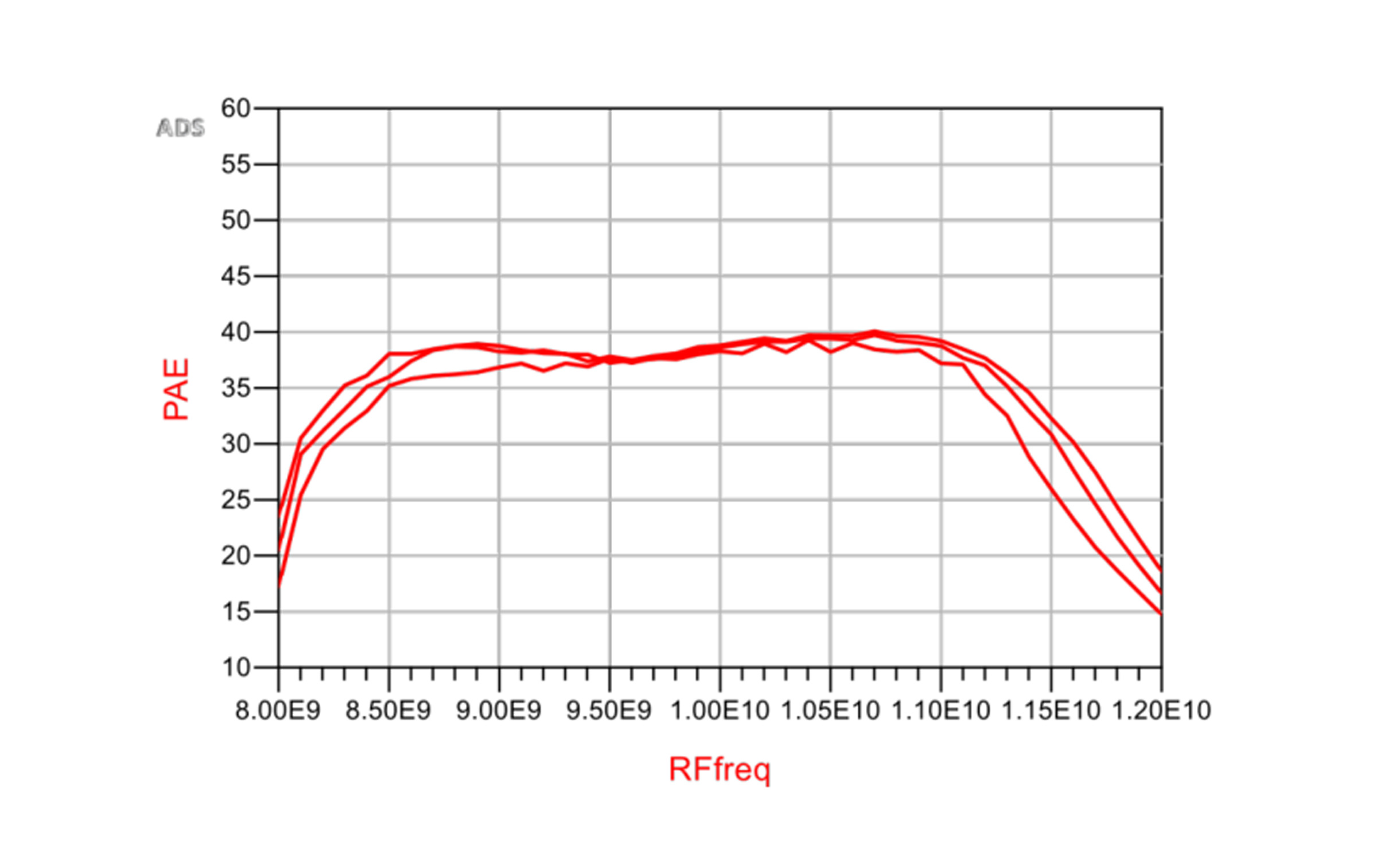
FIG, 1 Power additional efficiency PAE curve with frequency
FIG. 1 shows the saturation output power additional efficiency PAE curvewith frequency at high and low temperatures. It can be seen from the figure that
PAE of the power amplifier is greater than 35% at all three temperatures.
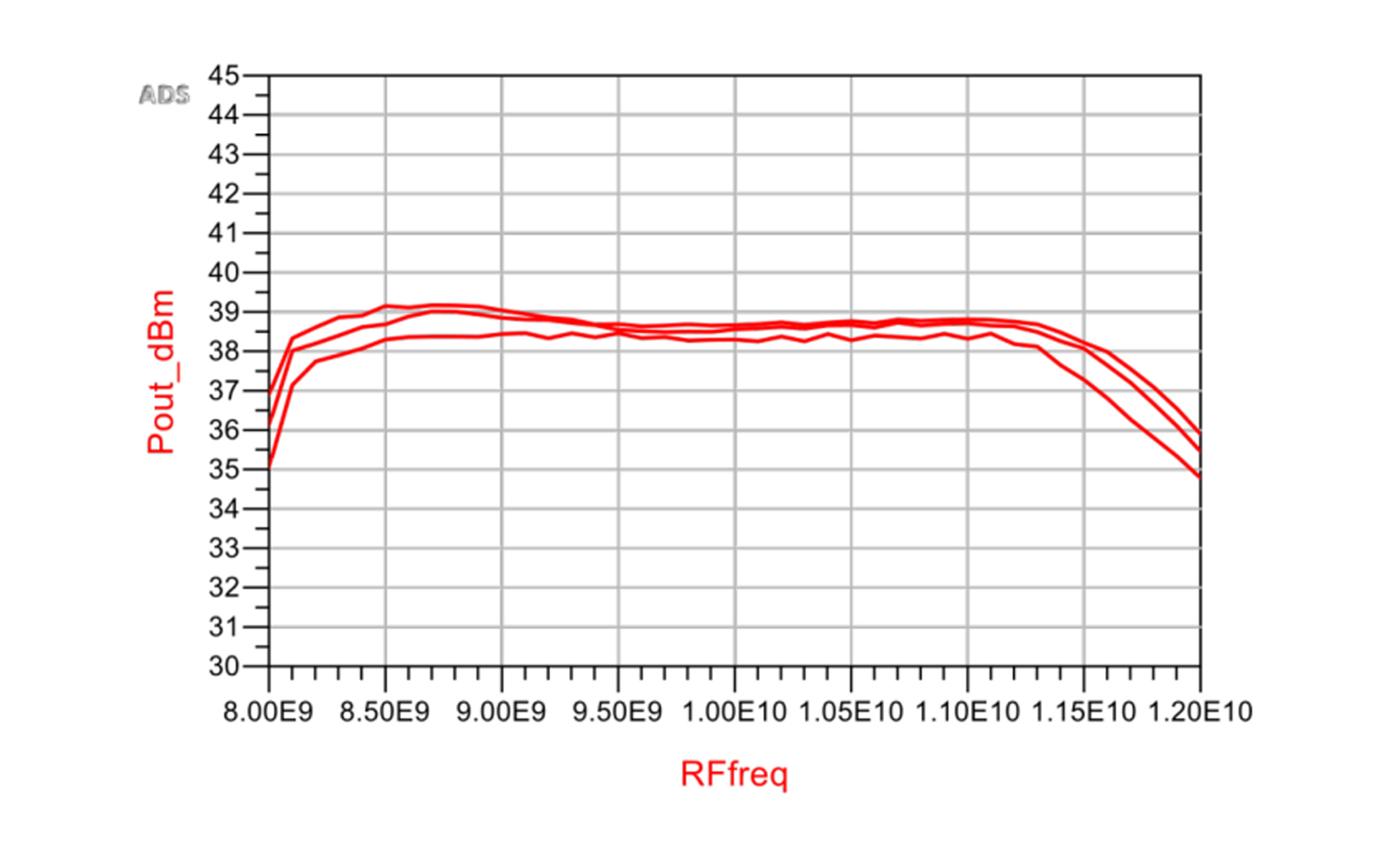
FIG.2 Saturation output power variation curve with frequency
FIG, 2 shows the saturation output power of the power amplifier changingwith frequency at high and low temperatures, It can be seen from the figure thatthe saturation output power of the power amplifier is greater than 38dBm atthree temperatures.
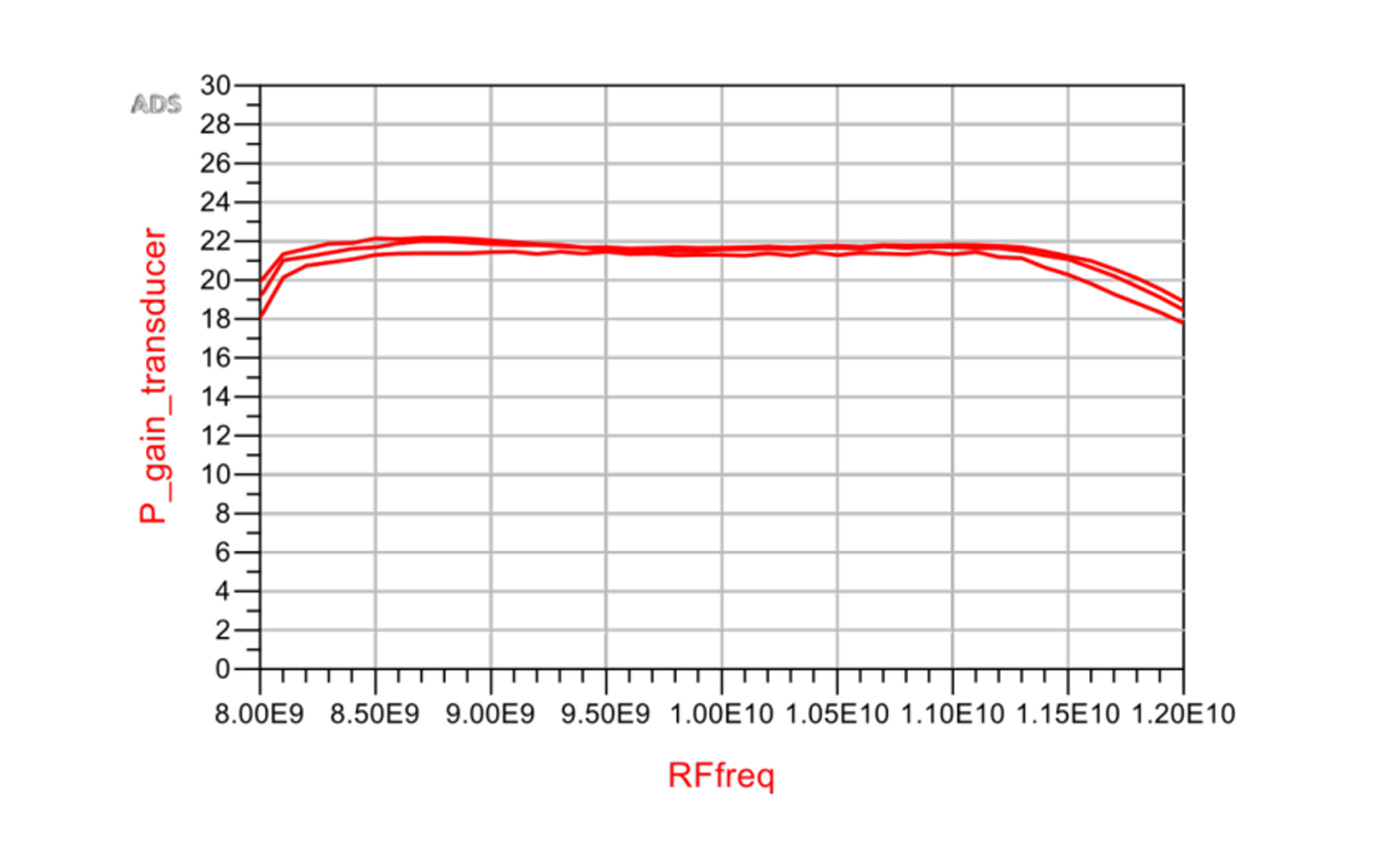
FIG. 3 Power gain variation curve with frequency
FIG. 3 shows the variation curve of power gain of the power amplifier withfrequency at high and low temperatures. It can be seen from the figure that thesaturation output power of the power amplifier is greater than 2ldB at threetemperatures.
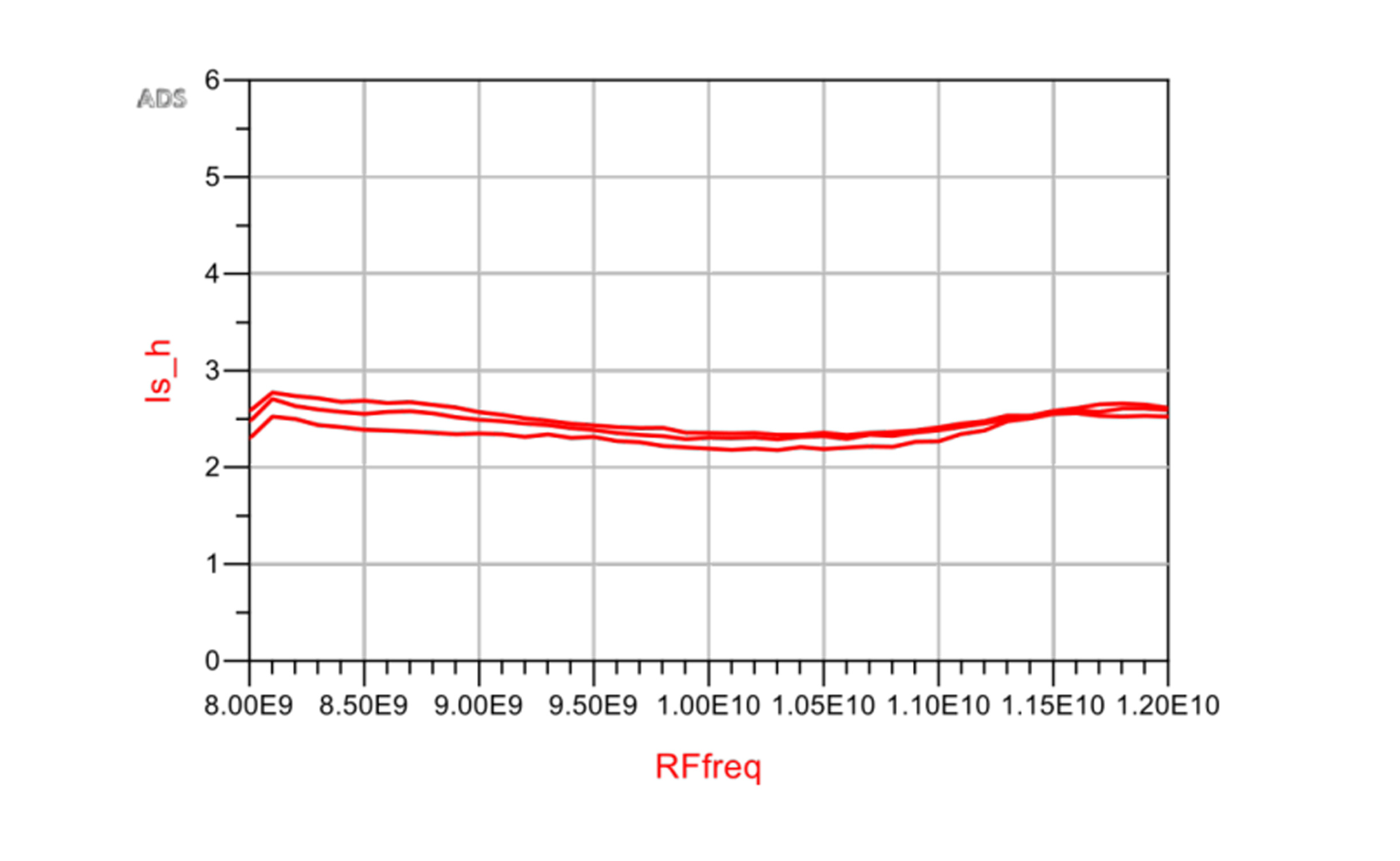
FIG. 4 Drain current variation curve with frequency
FIG. 4 shows the drain current curve of power amplifier with frequency athigh and low temperatures, It can be seen from the figure that at threetemperatures, the drain current of power amplifier is about 2.5A.
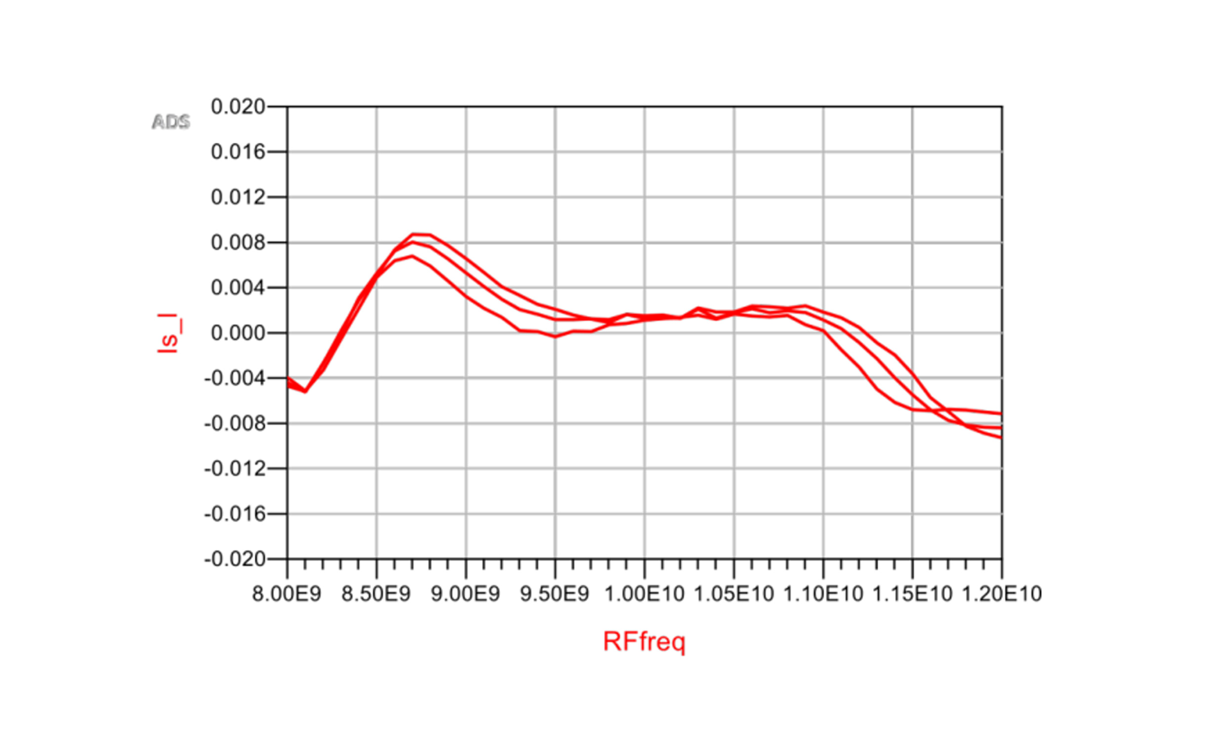
FIG. 5 Grid current change curve with frequency
FIG. 5 shows the change curve of the grid current of the power amplifierwith frequency at high and low temperatures, It can be seen from the figure thatthe grid current of the power amplifier is less than 8mA at three temperatures.
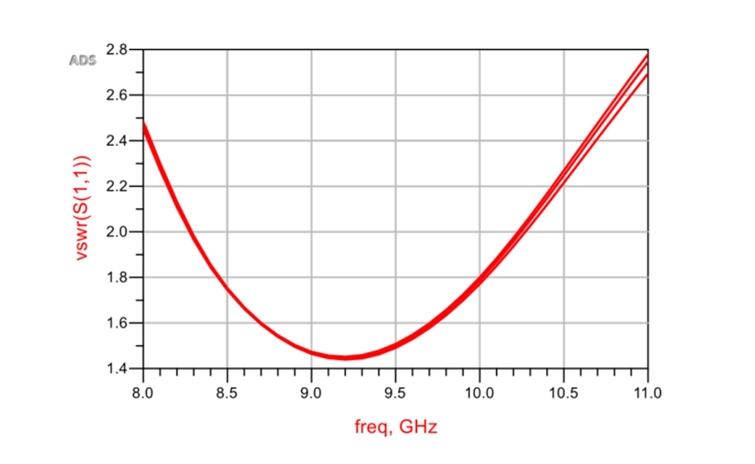
FIG, 6 Input standing wave coefficient variation curve with frequency
Figure 6 shows the variation curve of the input standing wave coefficient ofthe power amplifier with frequency under the condition of high and lowtemperature. It can be seen from the figure that under the condition of threetemperatures, the input standing wave coefficient of the power amplifier in theworking band is less than 1.8.
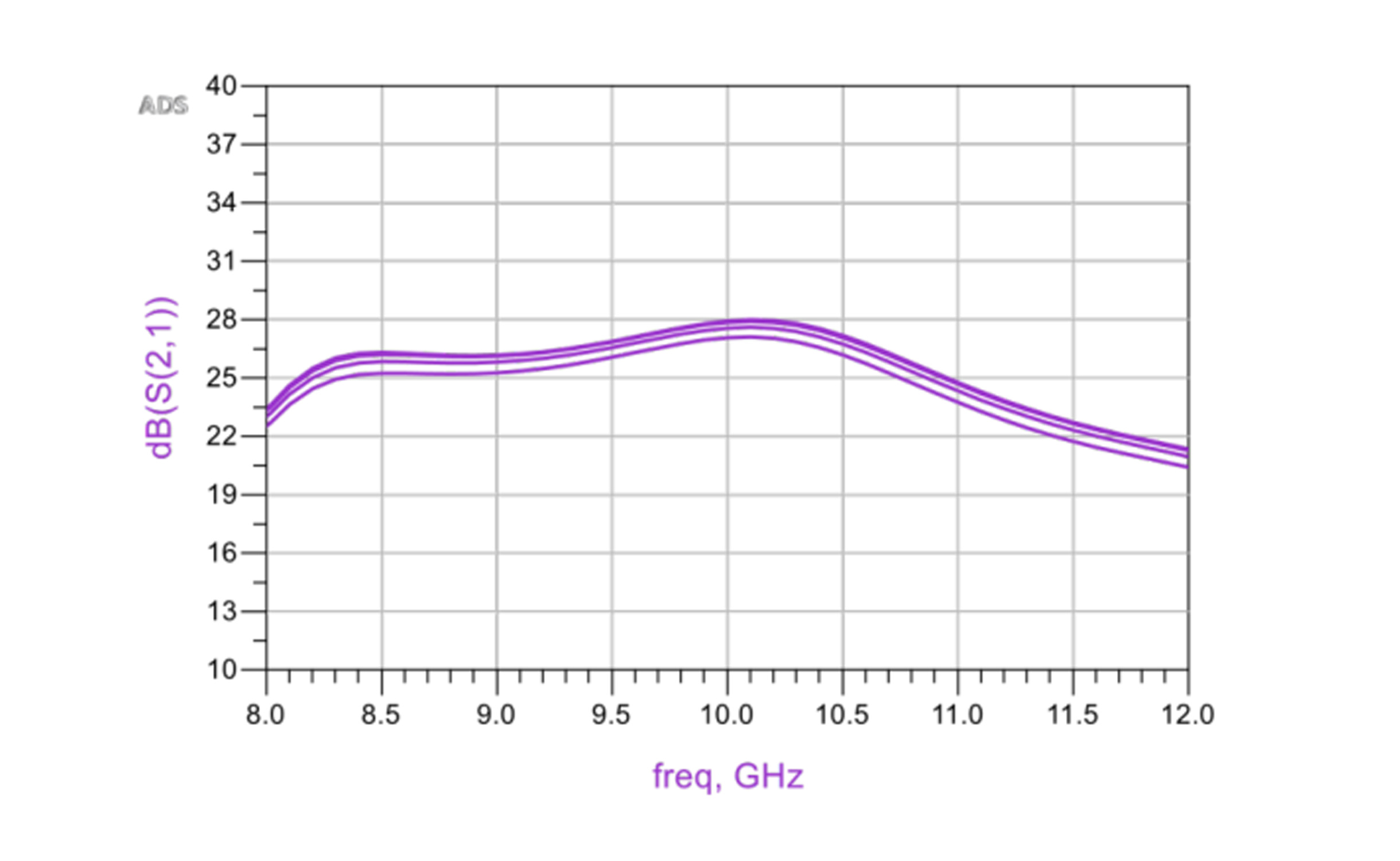
FIG. 7Curve ofS2l with frequency
FIG.7 shows the frequency variation curve of power amplifier S2l at highand low temperatures, It can be seen from the figure that in the threetemperature condition, the power amplifier S2l is within the range of 25~28dBin the working band, and deteriorates with the increase of temperature.
Chip size
Chip size nominal values and bonding area locations are shown below in μm.
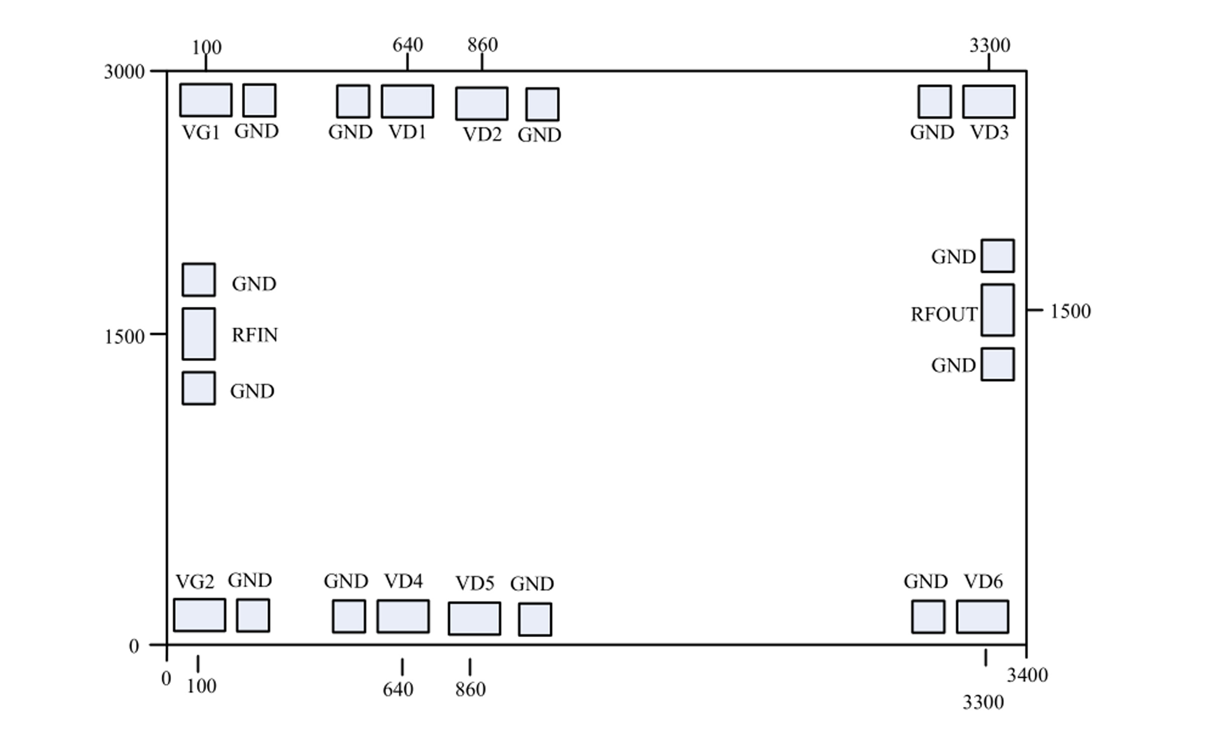
Exit terminal definition
| Symbol | Features |
Dimensions(mm2) |
| VD1/VD2/VD3/VD4/VDS/VD6 | Drain voltage plus bonding point | 150*100 |
| RFin | Microwave input signal bonding point | 150*100 |
| RFout | Microwave output signal bonding point | 150*100 |
| GND | Microwave ground point | 150*100 |
| VG1/VG2 | Grid bias voltage | 150*100 |
Previous
Next
Inquire Now
Note: Please leave your email address, our professionals will contact you as soon as possible!
Related Products