
Products
Related Posts
What is
GA 4667a
?

Category:


7-20GHz Medium
PowerAmplifier
GaAs Monolithic MicrowaveICinSMDpackage
Description
The KP 4667a is a wide band monolithic medium power amplifier.It is designed for a wide range of applications, from military to commercial communication systems
It is ESD protected on RF ports thanks to DCspecific filter circuits.
It is available in lead-free SMD package.
Main Features
● Broadband performance 7-20.5GHz
● Self-biased
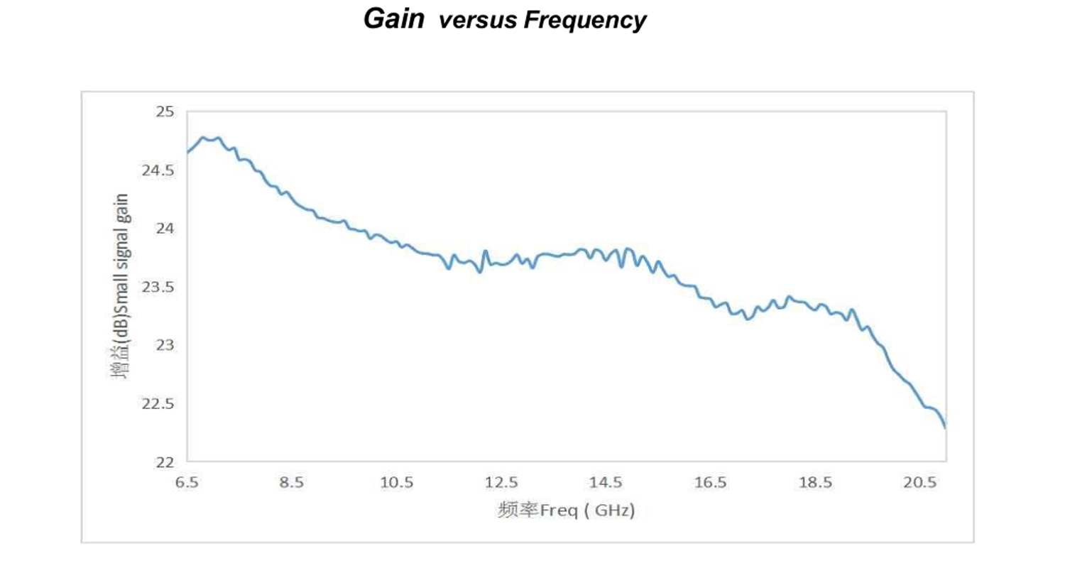
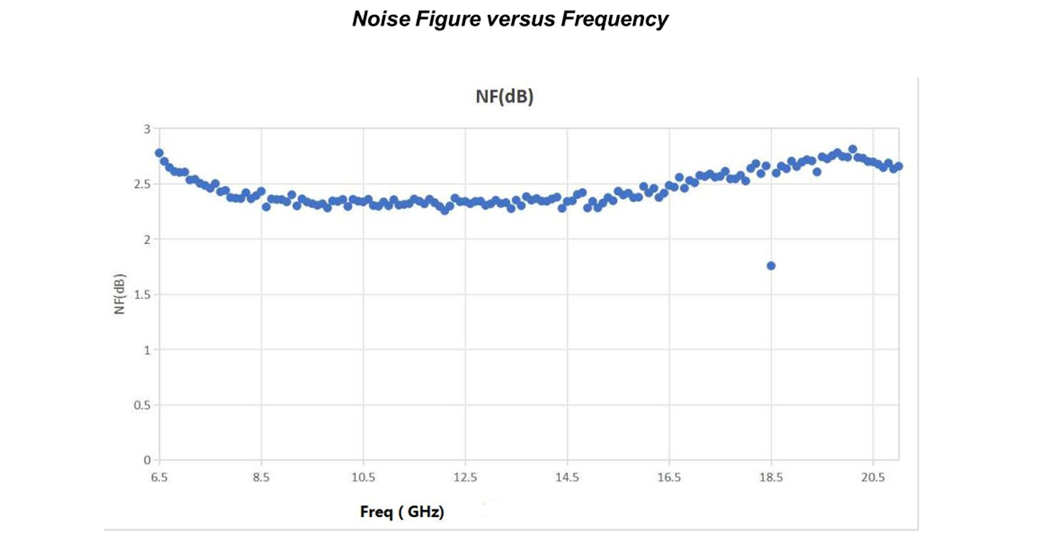
● 24dB gain @2.5dB noise figure
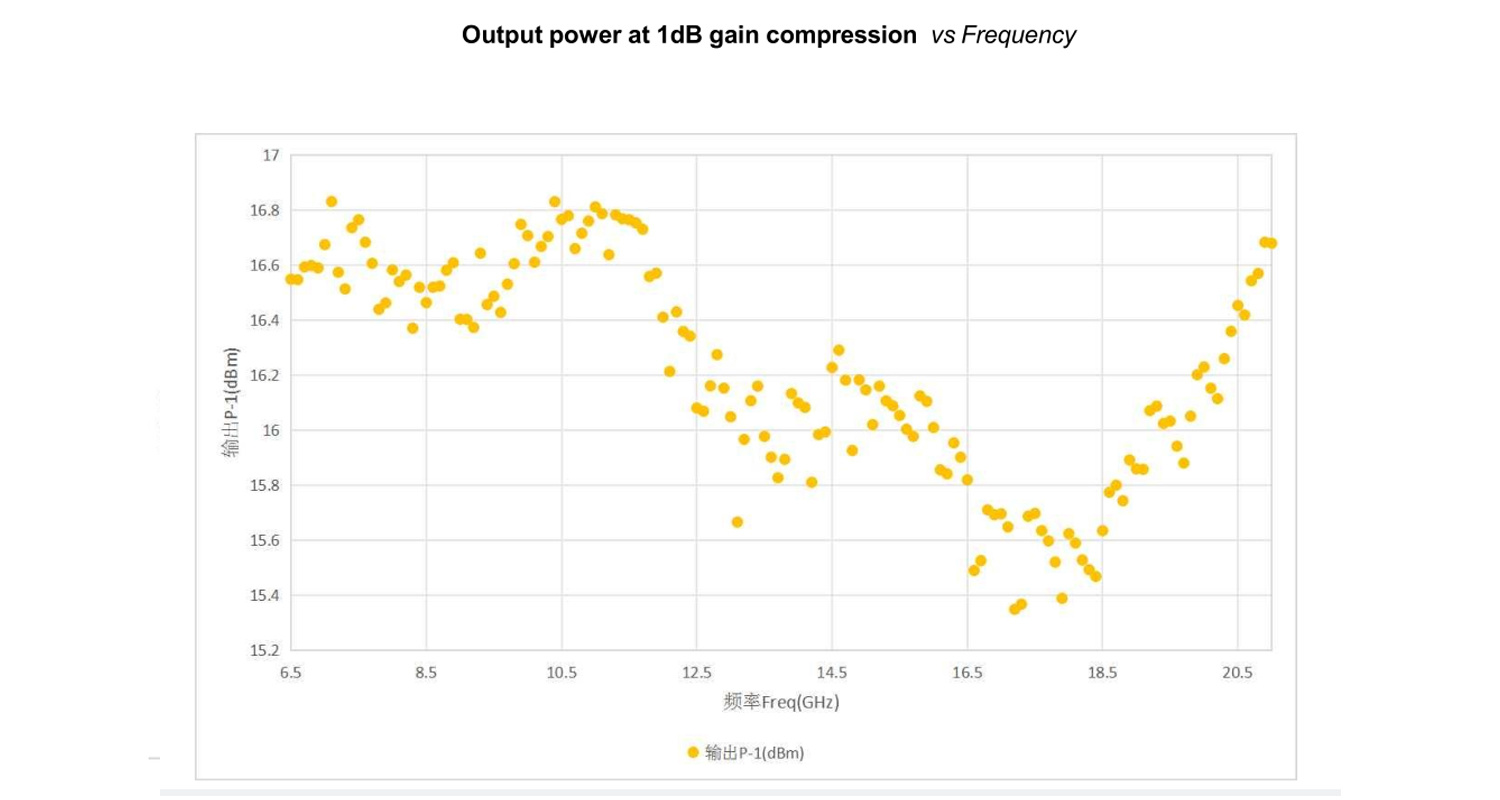
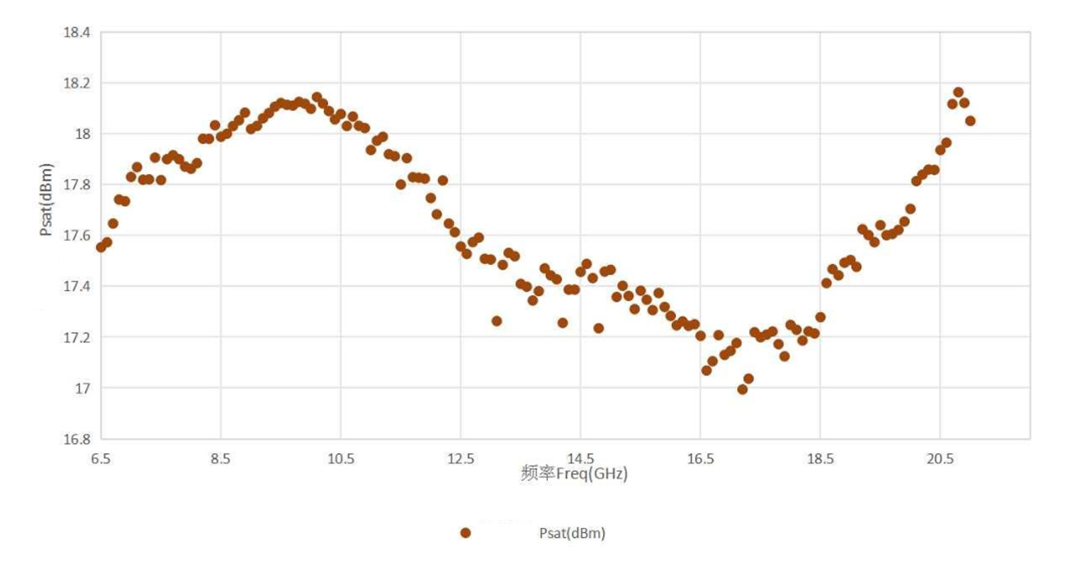
● 17.5dBm Output power@1dB compression
● DC power consumption, 120 mA @4.2V
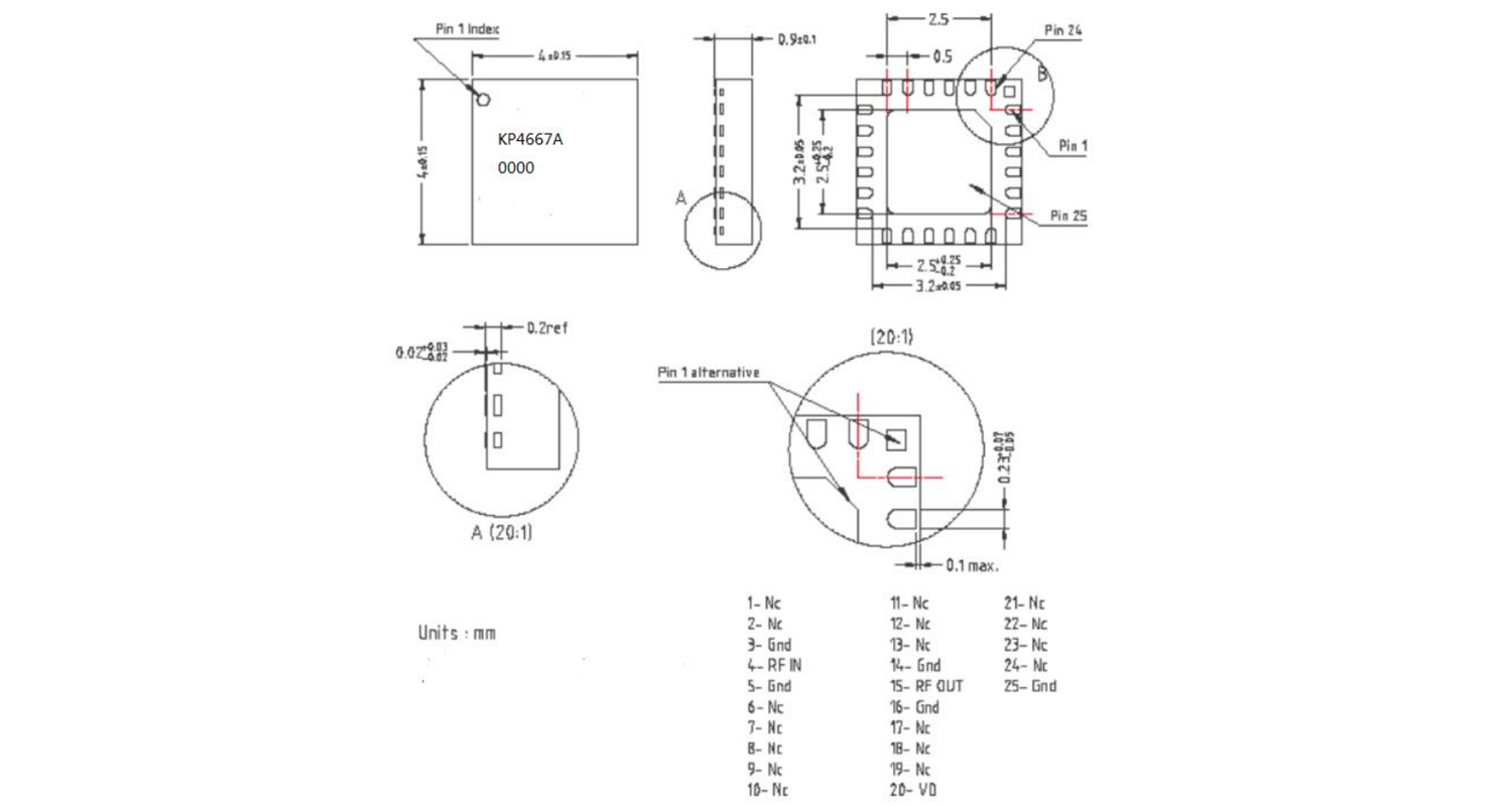
● 24L-QFN4X4 SMD package(Ceramic package)
● ESD protected
Main Characteristics
Tamb.=25°C,Vd= 4.2V
| Symbol | Parameter | Min | Typ | Max | Unit |
| Fop | Input frequency range | 7 | 20 | GHz | |
| G | Small signalgain | 22.7 | 24 | 24.7 | dB |
| NF | Noise Figure | 2.2 | 2.5 | 2.7 | dB |
| P-1dB | Output power at1dB gain compression | 17 | 17.5 | 18 | dBm |
| ld | Bias current | 70 | 120 | 135 | mA |
Electrical Characteristics
Tamb.=25°C,Vd=4.2V
| Symbol | Parameter | Min | Typ | Max | Unit |
| Fop | Operating frequencyrange | 7 | 20.2 | GHz | |
| G | Gain (7-9GHz) (9-17GHz) (17-20GHz) |
24.6 23.4 23.1 |
dB | ||
| NF | Noisefigure(7-18 GHz) | 2.7 | dB | ||
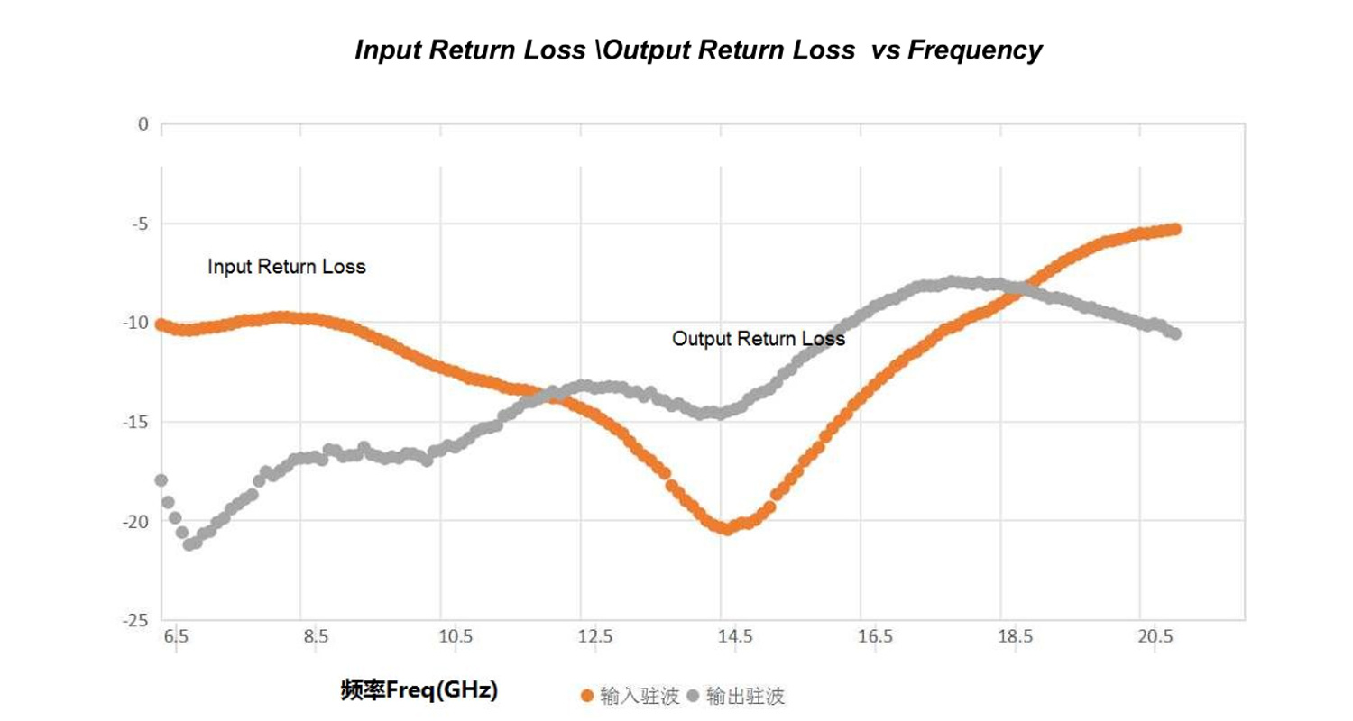
| RLin | InputReturn Loss | -10 | dB | ||
| RLout | OutputReturn Loss | -15 | dB | ||
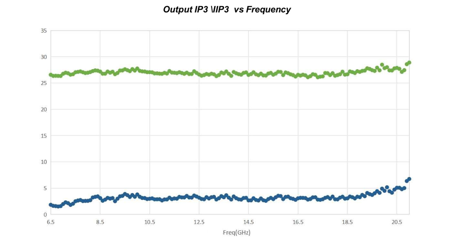
| IP3 | OutputIP3 | 26 | dBm | ||
| P-1dB |
Pout at 1dB gain compression (7-13 GHz) |
17.5 16.8 |
dBm dBm |
||
| lsol | Reverseisolation | 40 | dB | ||
| Vd | Drain bias voltage | 4.2 | V | ||
| ld | Drain bias current | 120 | mA |
Absolute Maximum Ratings(1)
Tamb=+25°C
| Symbol | Parameter | Values | Unit |
| Vd | Drain bias voltage | 5V | V |
| ld | Powersupply quiescent current | 135 | mA |
| Pin | RF input power(2) | 18 | dBm |
| Top | Operating temperature range | -40 to +85 | °C |
| Tj | Junction temperature(3) | 175 | °C |
| Tstg | Storage temperature range | -55 to +125 | °C |
Typical Measured Performance
Tamb=+25°C,Vd=+4.2VId=120mA
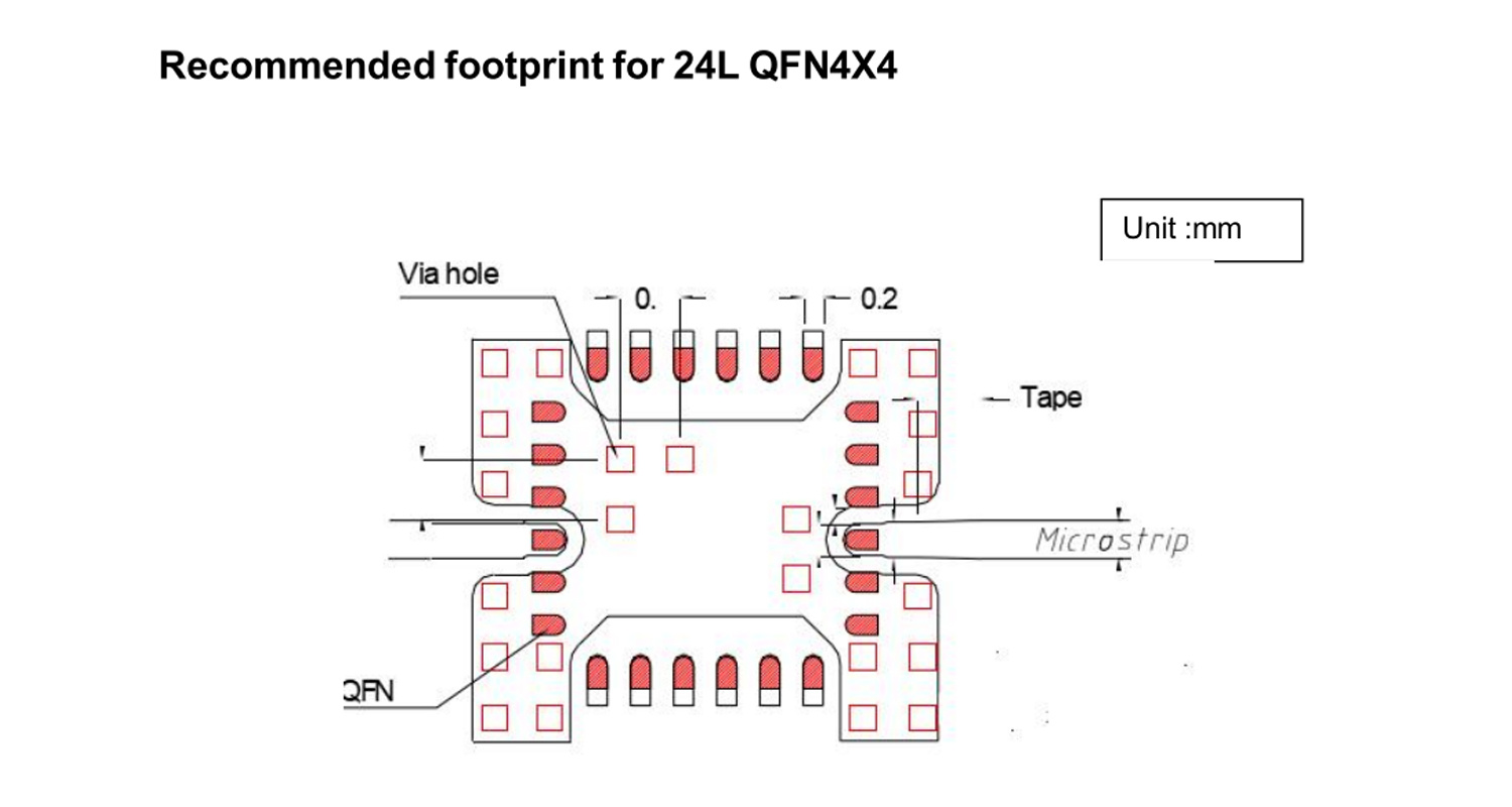
Package outline
Previous
Next
Inquire Now
Note: Please leave your email address, our professionals will contact you as soon as possible!
Related Products