
Products
Related Posts
What is
GA6061
?

Category:


FEATURES
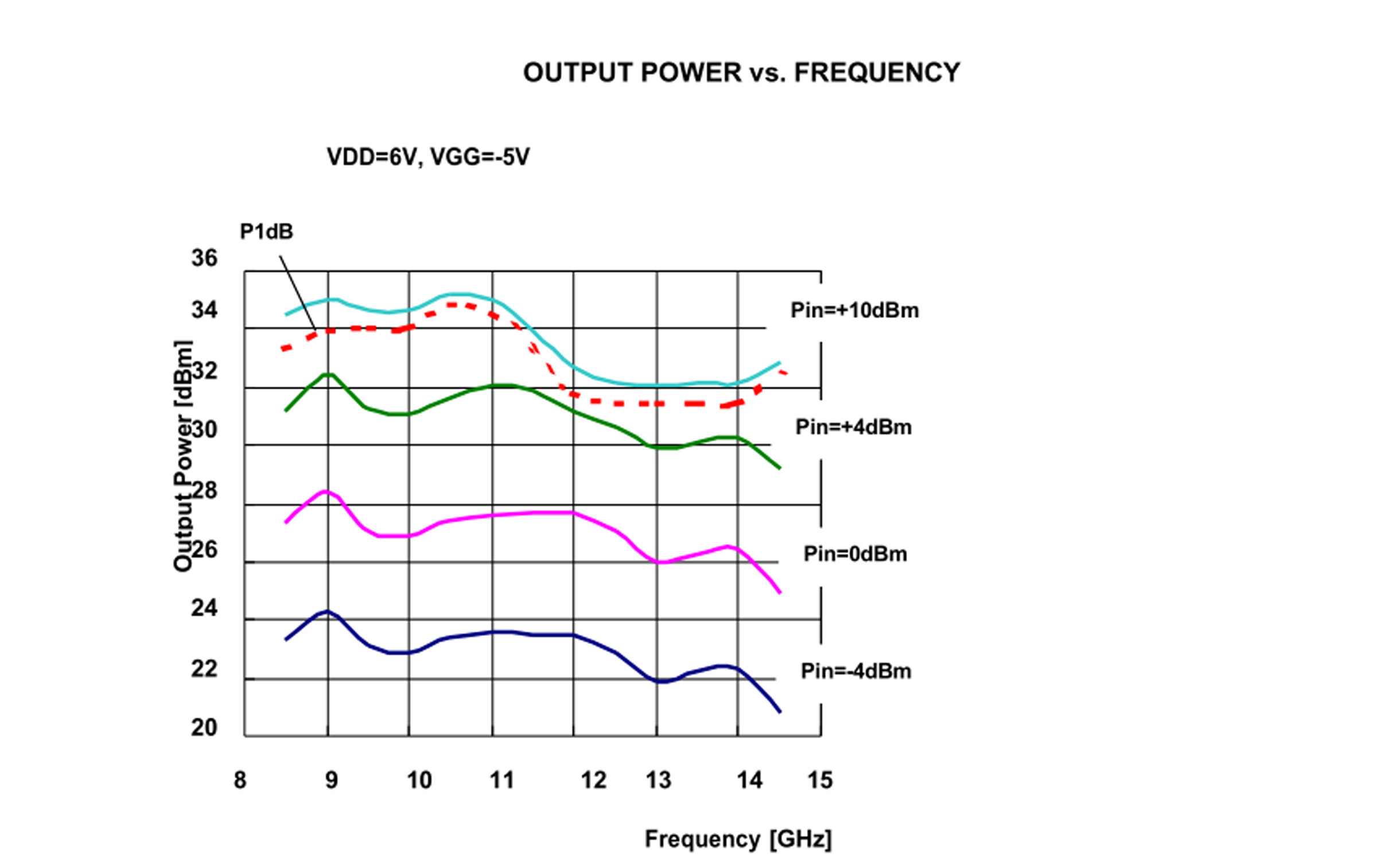
● High Output Power: Pout=34.0dBm (MAX.)
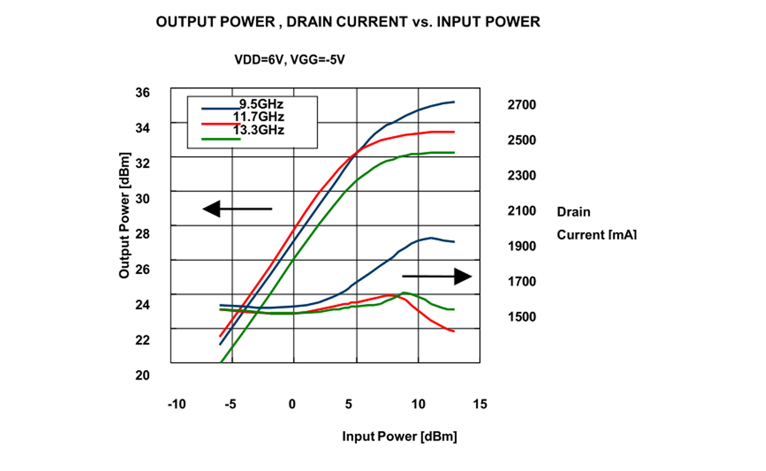
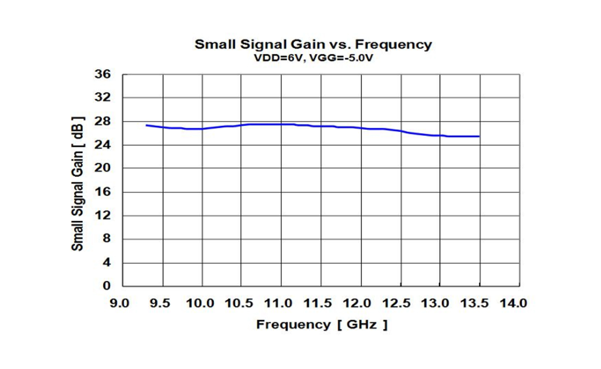
● High Linear Gain: GL=27.0dB (typ.)
● Broad Band:9.5~13.5GHz
● Impedance Matched Zin/Zout=50Ω
● Small Hermetic Metal-Ceramic Package(VF)
DESCRIPTION
The KP 6061VF is a MMlC amplifier that contains a three-stage amplifier,internally matched, for standard communications band in the9.5 to13.5GHzfrequency range.
ABSOLUTE MAXIMUM RATING
| ltem | Symbol | Condition | Rating | Unit |
| Drain-Source Voltage | VDD | 10 | V | |
| Gate-Source Voltage | VGG | 26 | V | |
| Input Power | Pin | -7 | dBm | |
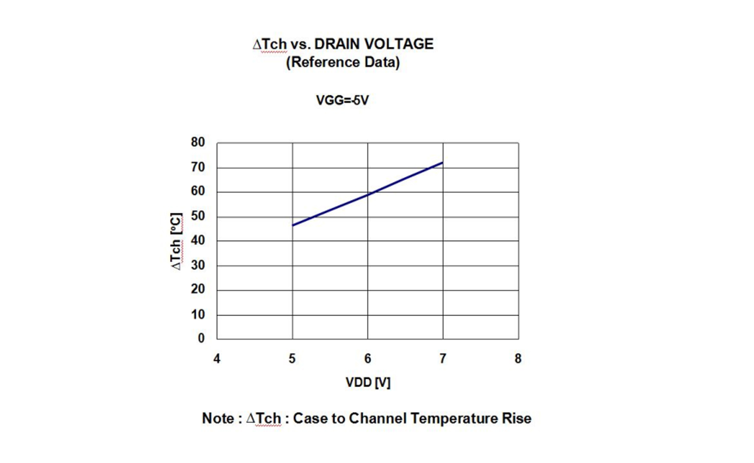
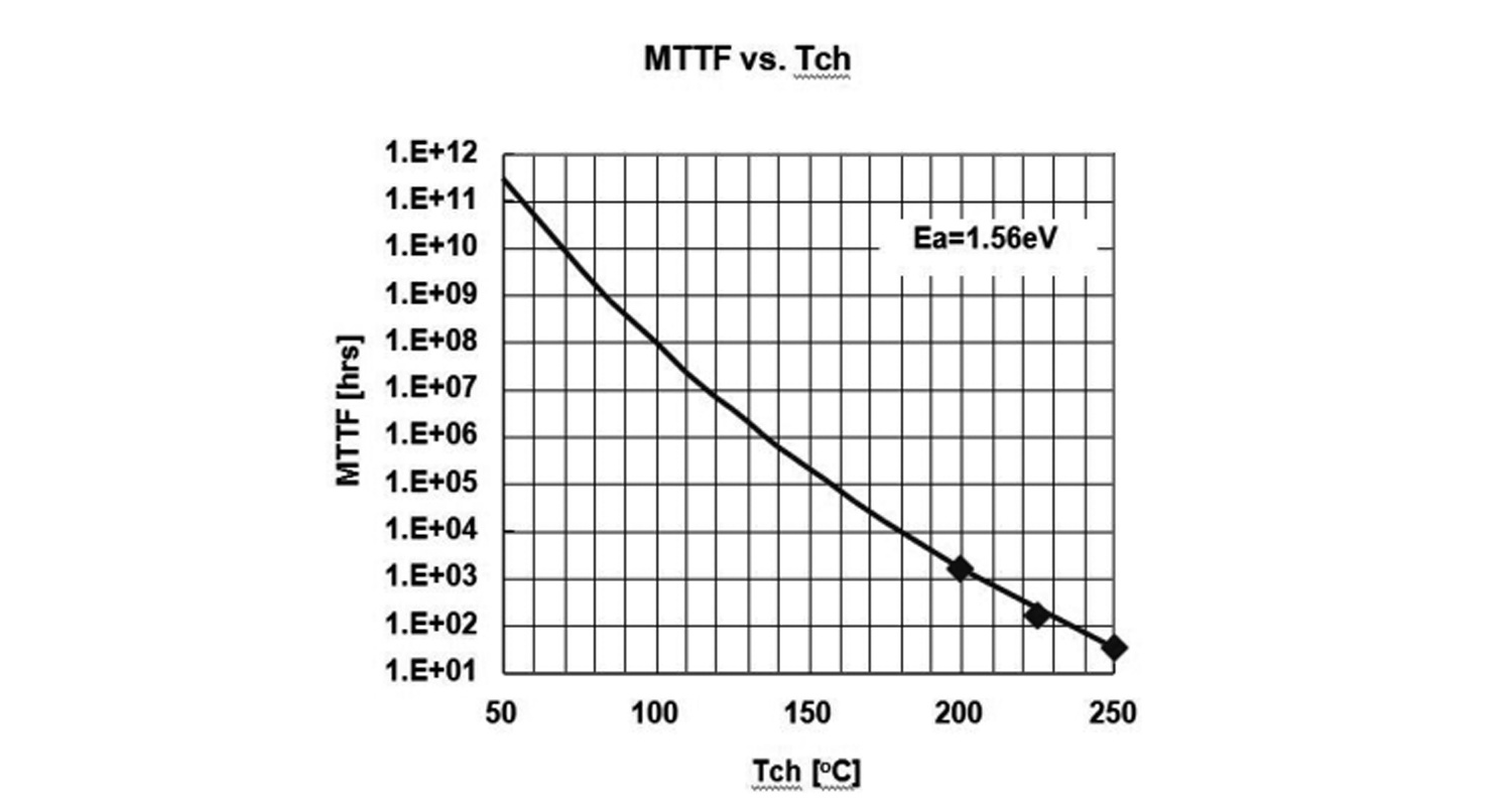
| Channel Temperature | TCH | +175 | ℃ | |
| Storage Temperature | Tstg | -55~125 | ℃ |
RECOMMENDED OPERATING CONDITION
| ltem | Symbol | Condition | Rating | Unit |
| Drain-Source Voltage | VDD | 6 | V | |
| Gate-Source Voltage | VGG | -5 | V | |
| Input Power | Pin | ≤y12 | dBm | |
| Operating Case Temperature | TC | -40~+85 | ℃ |
ELECTRICALCHARACTERISTICS(Case Temperature Tc=25°C)
| ltem | Symbol | test Condition | Limits | Unit | ||
| Min. | TyP. | Max. | ||||
| FrequencyRange | f |
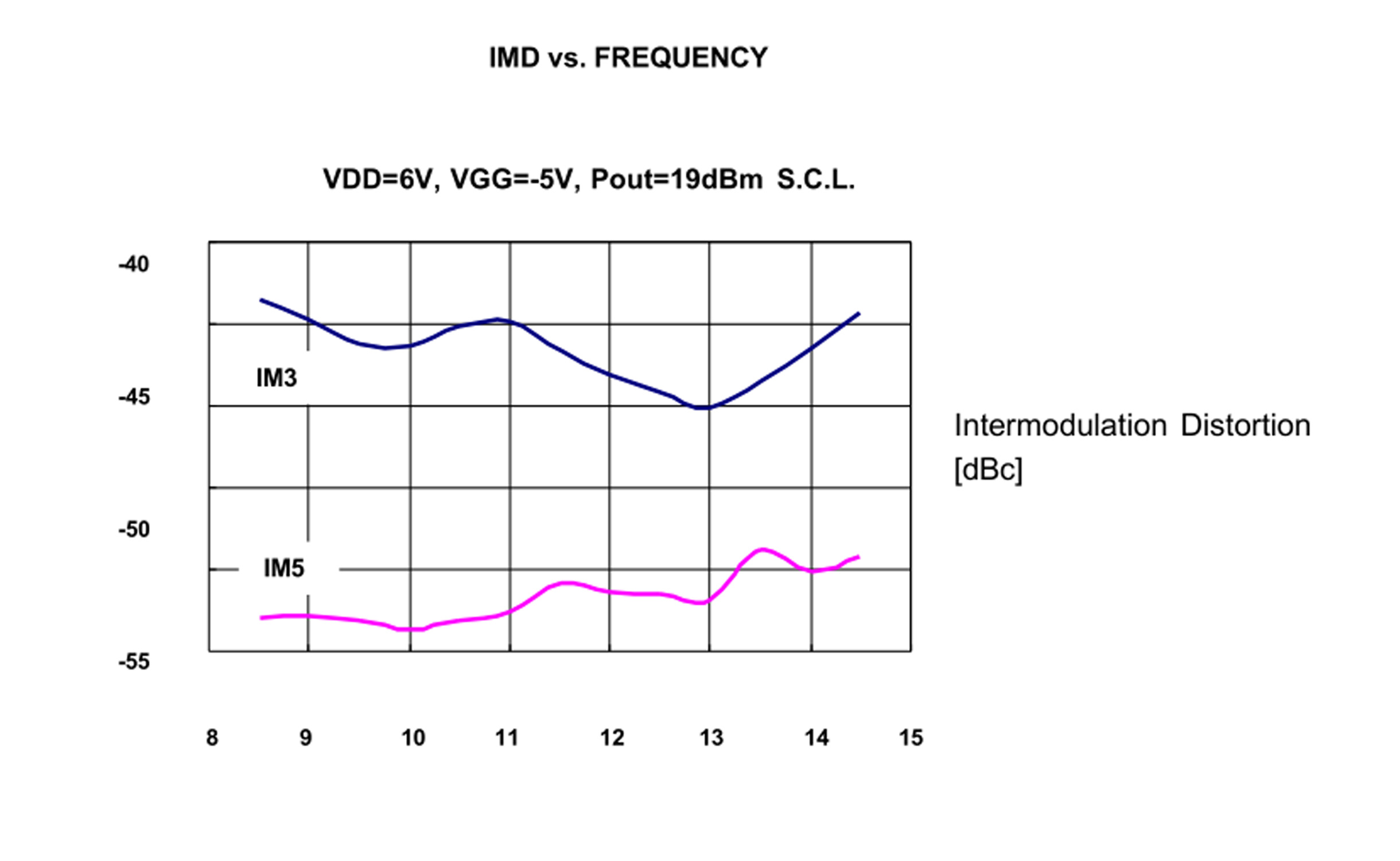
VDD=6V Zs=Z1=50ohm *1:f=9.5~11.7GHZ *2:f=11.7~13.3GHz *3:△f=10MHz, 2-Tone Test, Pout=19dBm S.C.L. ~199 V |
9.5 | - | 13.5 | GHz |
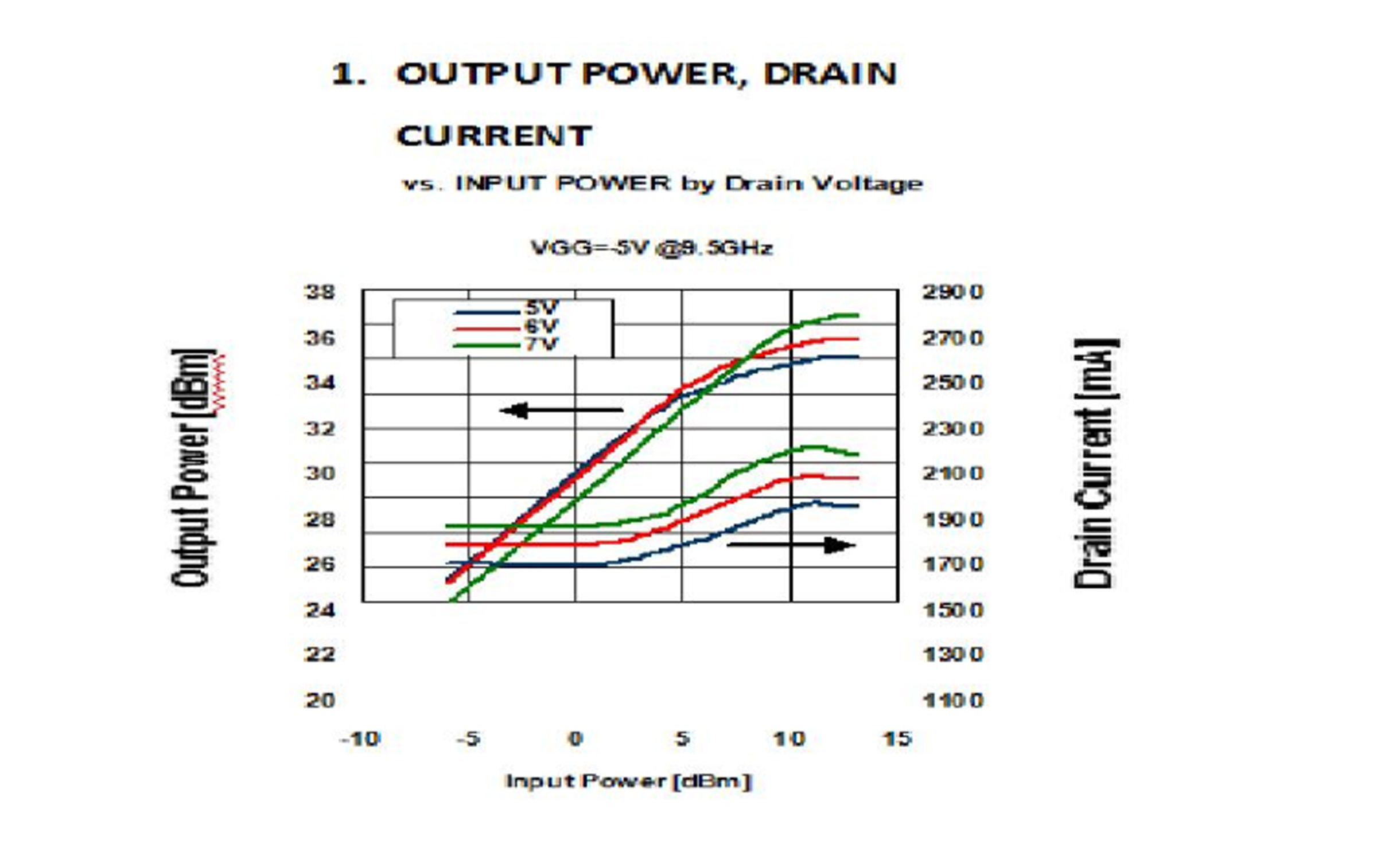
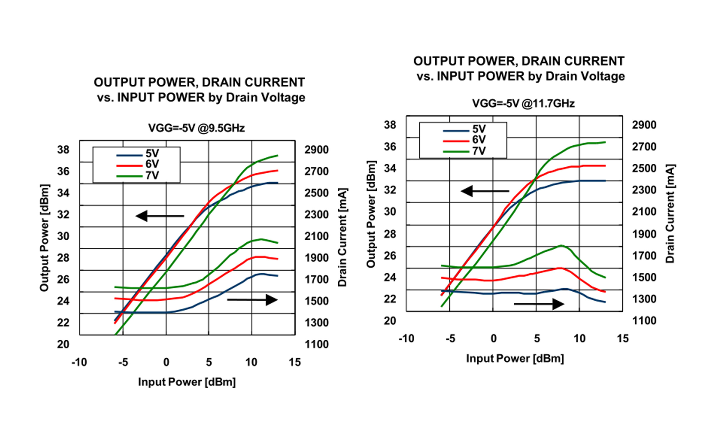
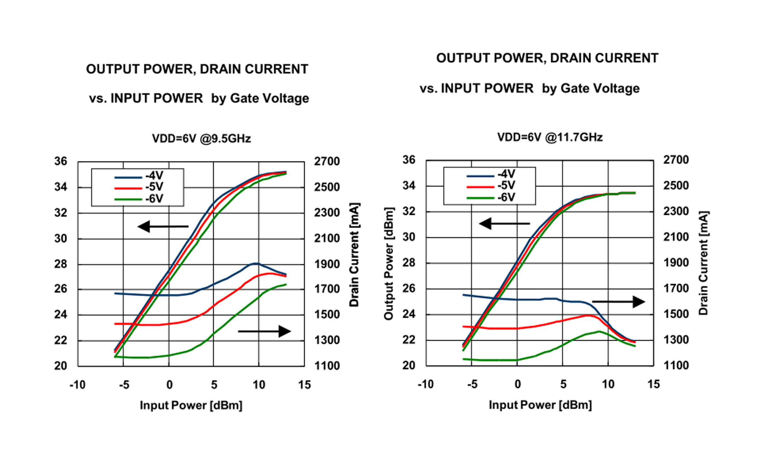
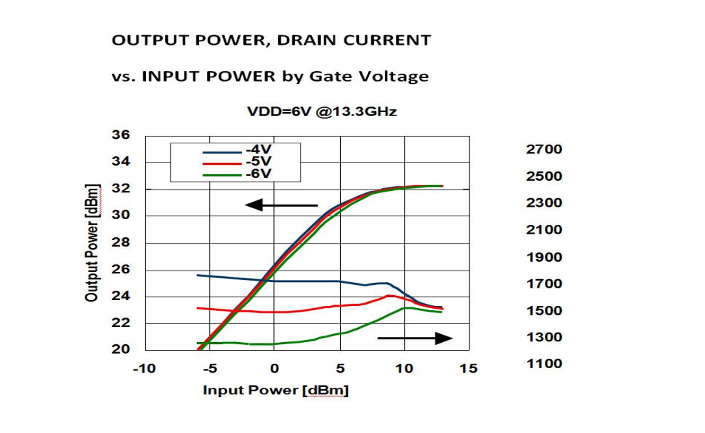
| Output Power at 1dB G.C.P | P1dB | 31*1 29*2 |
33*1 31*2 |
- - |
dBm | |
| Power Gain at 1dB G.C.P | G1dB | 24*1 22*2 |
26*1 24*2 |
- - |
dB | |
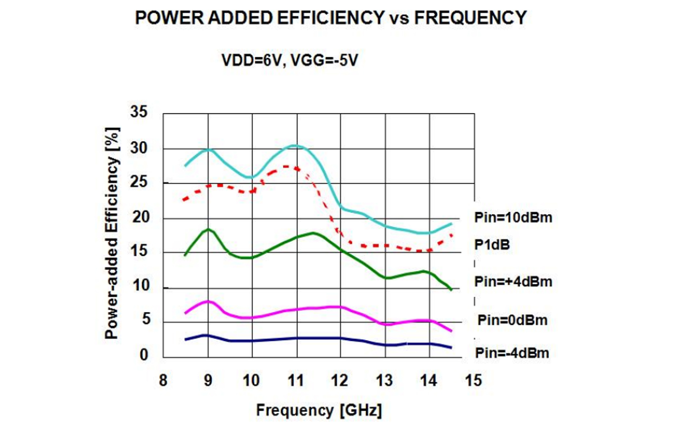
| Power-added Efficiency at 1dB G.C.P. | nadd |
- - |
21*1 15*2 |
- - |
% | |
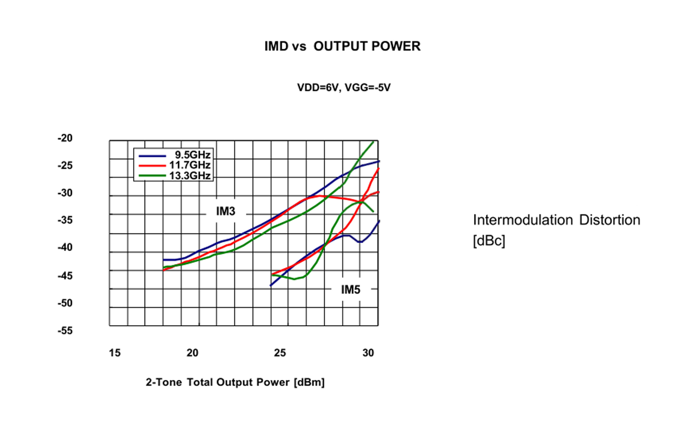
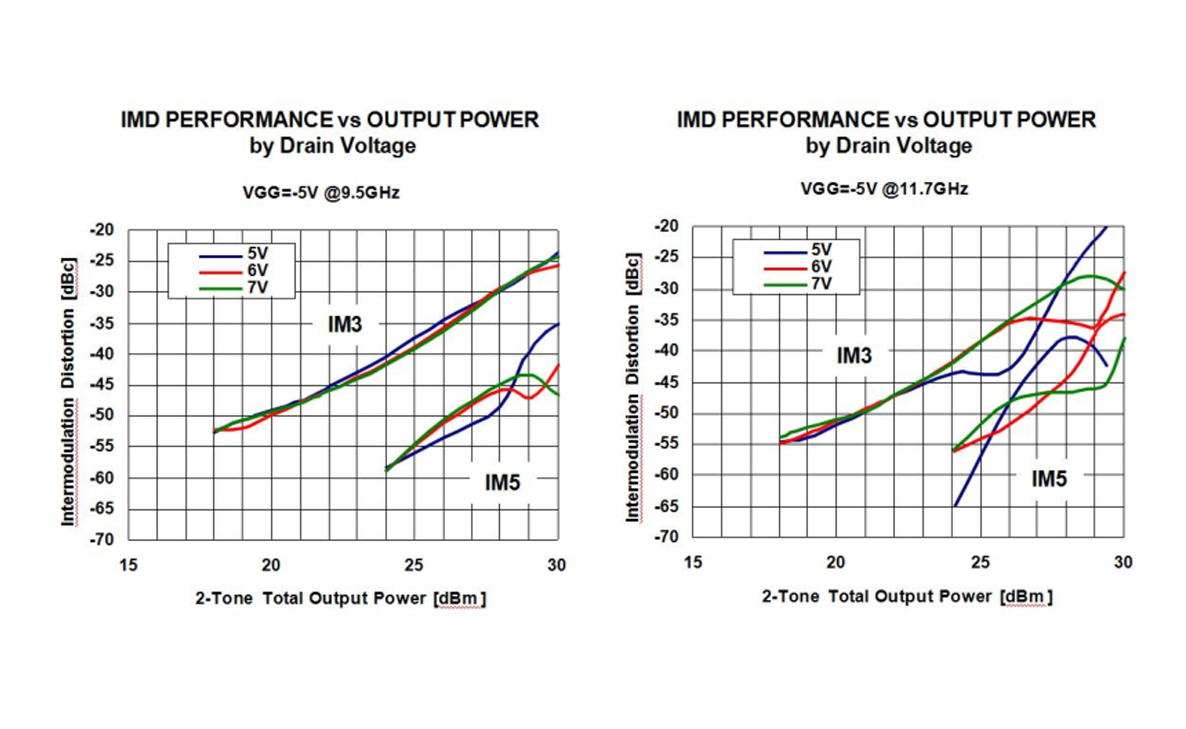
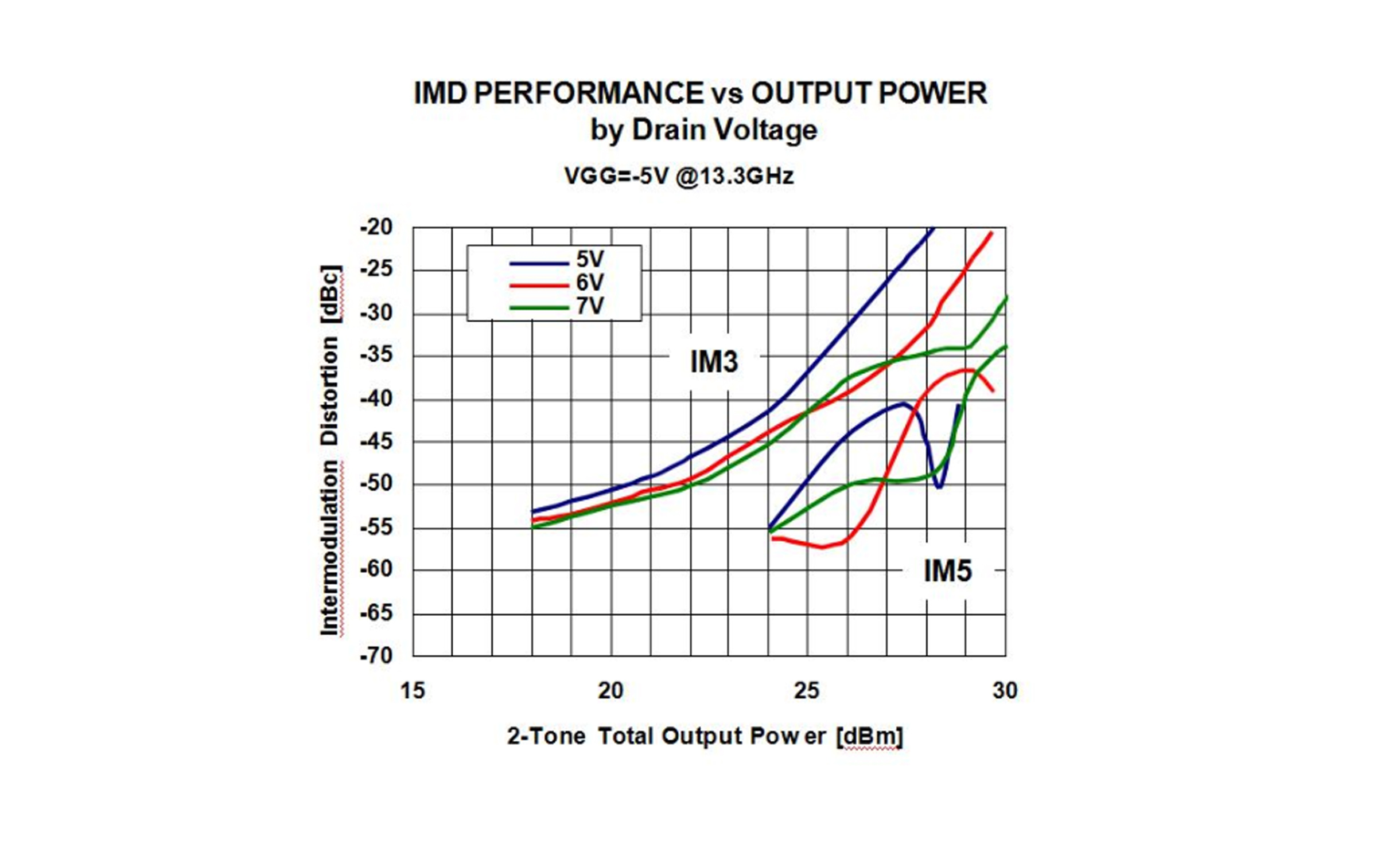
| Thge Sier intermodulation" | IM3 | -42*3 | -42*3 | - | dBc | |
| Drain Current at 1dB G.C.P. | Idd |
- - |
1700*1 1500*2 |
2400*1 2400*2 |
mA mA |
|
| Gate Current | IGG | - | 25 | - | mA | |
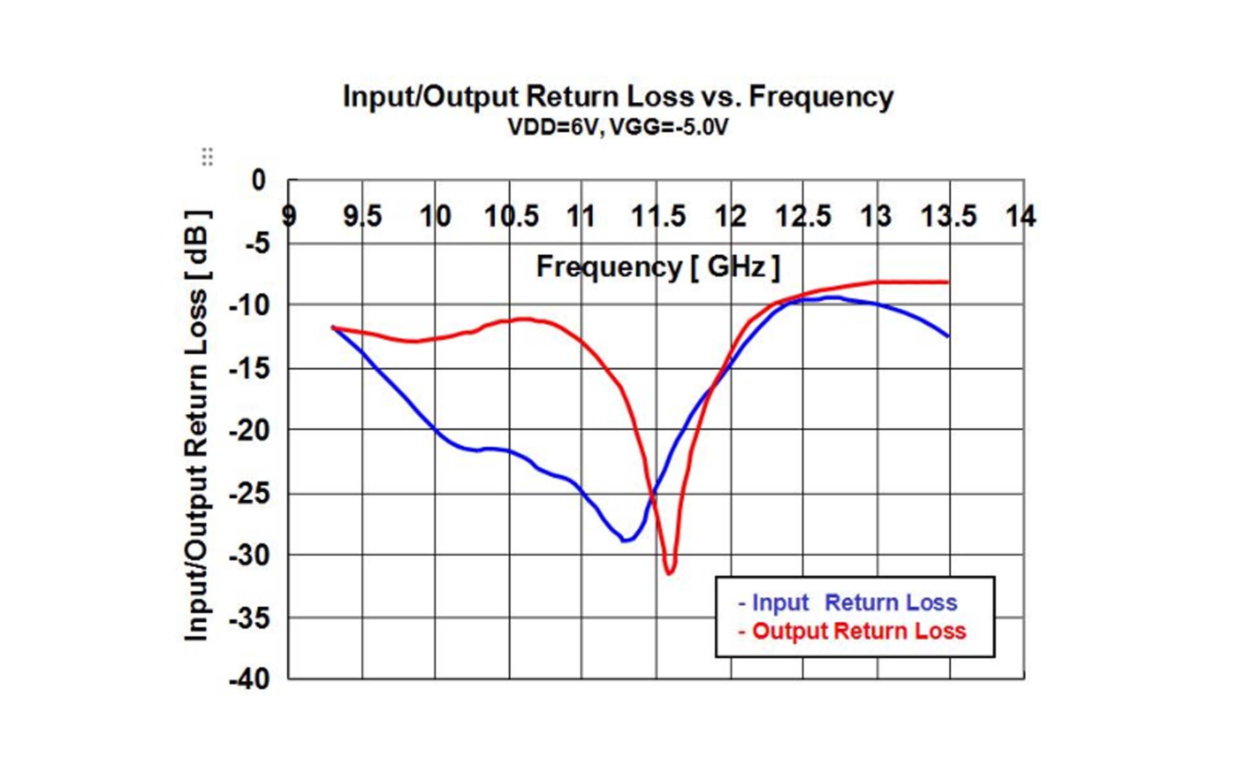
| Input Return Loss(at Pin=-20dBm) | RLin | - | -8 | - | dB | |
| Output Return Loss (at Pin=-20dBm) | RLout | - | -8 | - | dB | |
| ESD | Class 0 | |||||
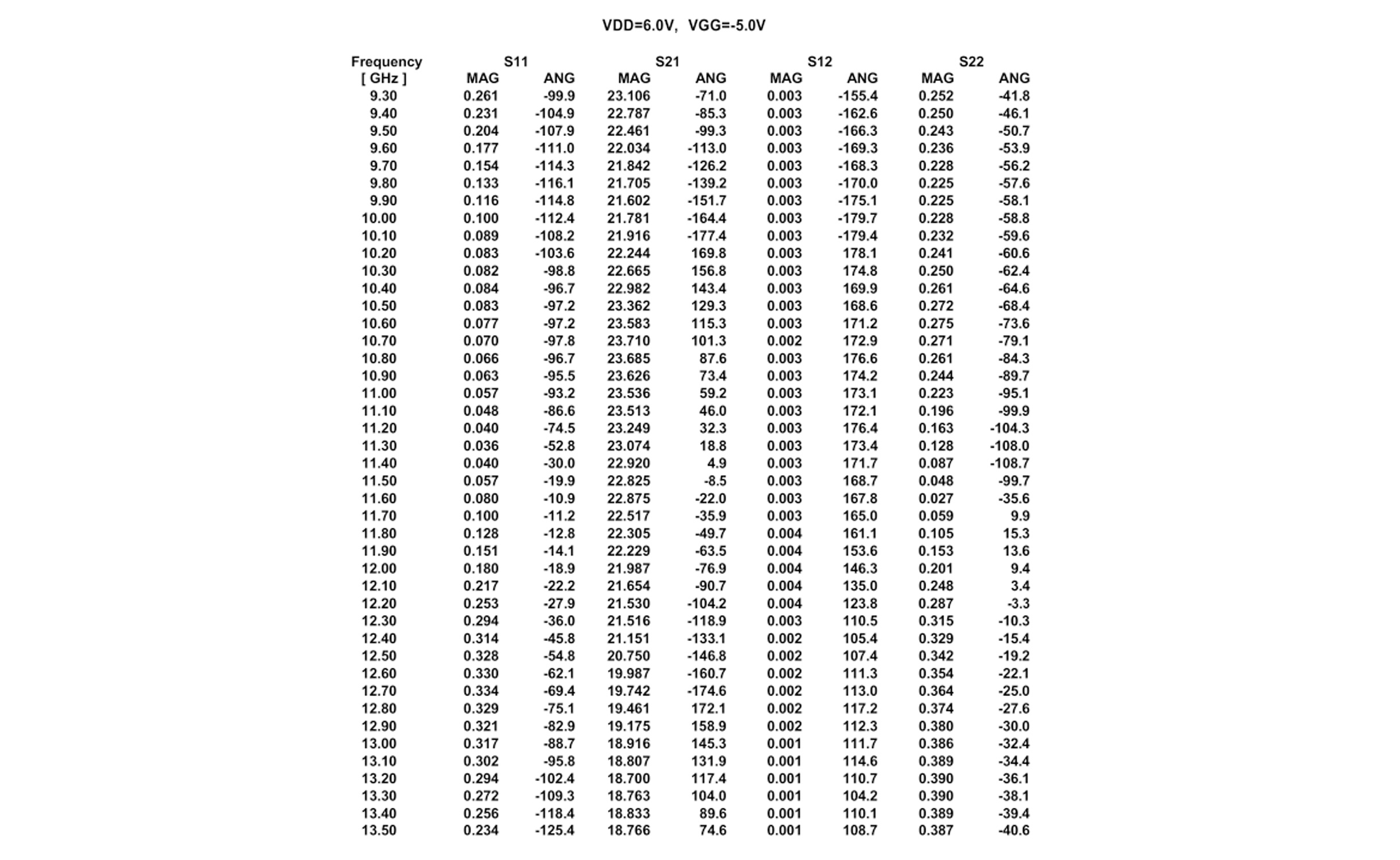
S-PARAMETER
Package Out Line
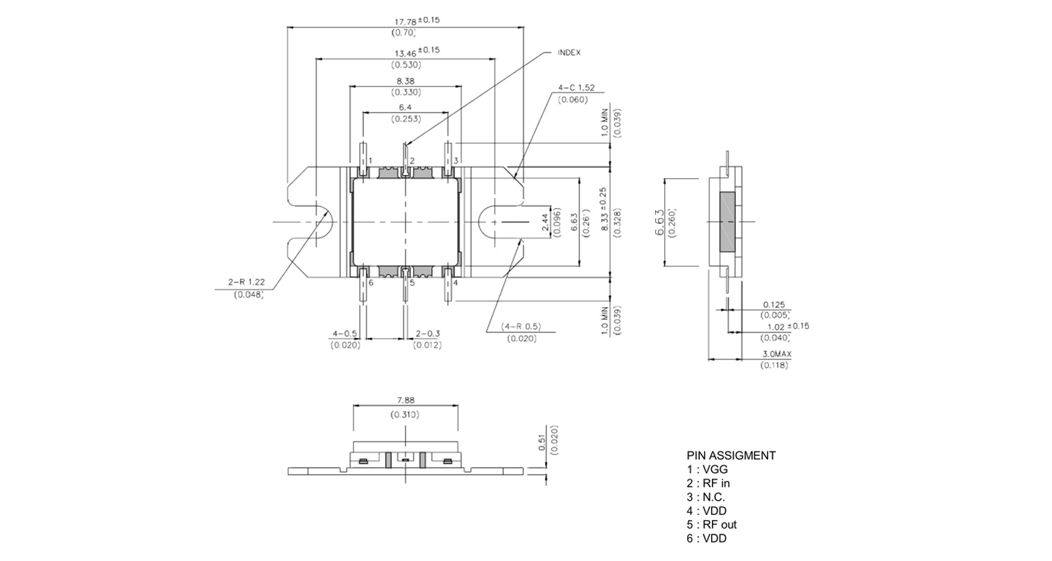
Mounting Instructions for VF Package
1.Screw Mounting
(1)The flange of package may be attached using screws. Torque conditionsare shown in table 1.
Table 1.Recommended and Maximum Torque for Screw Mounting
| Package | Recommended screw |
Recommended Torque |
Maximum Torque |
| VF | M2.0 | 10 N-cm (0.9 lb-in) | 15 N-cm (1.3 lb-in) |
(2)First, tighten the screws with a torque driver set to 5 N-cm.
(3)The surface finish of the heat sink should be better than 0.8m, and thesurface flatness must be better than 10 m.
(4)Silicon based heat sink compounds should not be used for thermalconductive grease. They cause poor grounding of the source flange,contamination and long term degradation of thermal resistance between theFET package and heat sink.
2.Solder Mounting
(1)Recommended solder are Tin-Lead solder (63Sn/37Pb), Lead-Freesolder (Sn-3.0Ag-0.5Cu)*1 or equivalent.
(2)For soldering,Tin-Lead solder(63Sn/37Pb)or Lead-Freesolder (Sn-3.0Ag-0.5Cu)*1 shall be used. (*1: The figure displays withweight %. A predominantly tin-rich alloy with 3.0% silver and 0.5% copper.)
(3)Recommended Flux is Rosin type with chlorine content: 0.2% or less anda low halogen content. After soldering, the flux residue should be removedby appropriate cleaning methods.
(4)The recommended soldering conditions are as follows: Partial heatingmethod (soldering iron, spot laser/air)Product terminal temperature: 260 deg-C, max. 10 s./terminalor 400 deg-Cmax. 3 s./terminal
Previous
Next
Inquire Now
Note: Please leave your email address, our professionals will contact you as soon as possible!
Related Products