
Products
Related Posts
What is
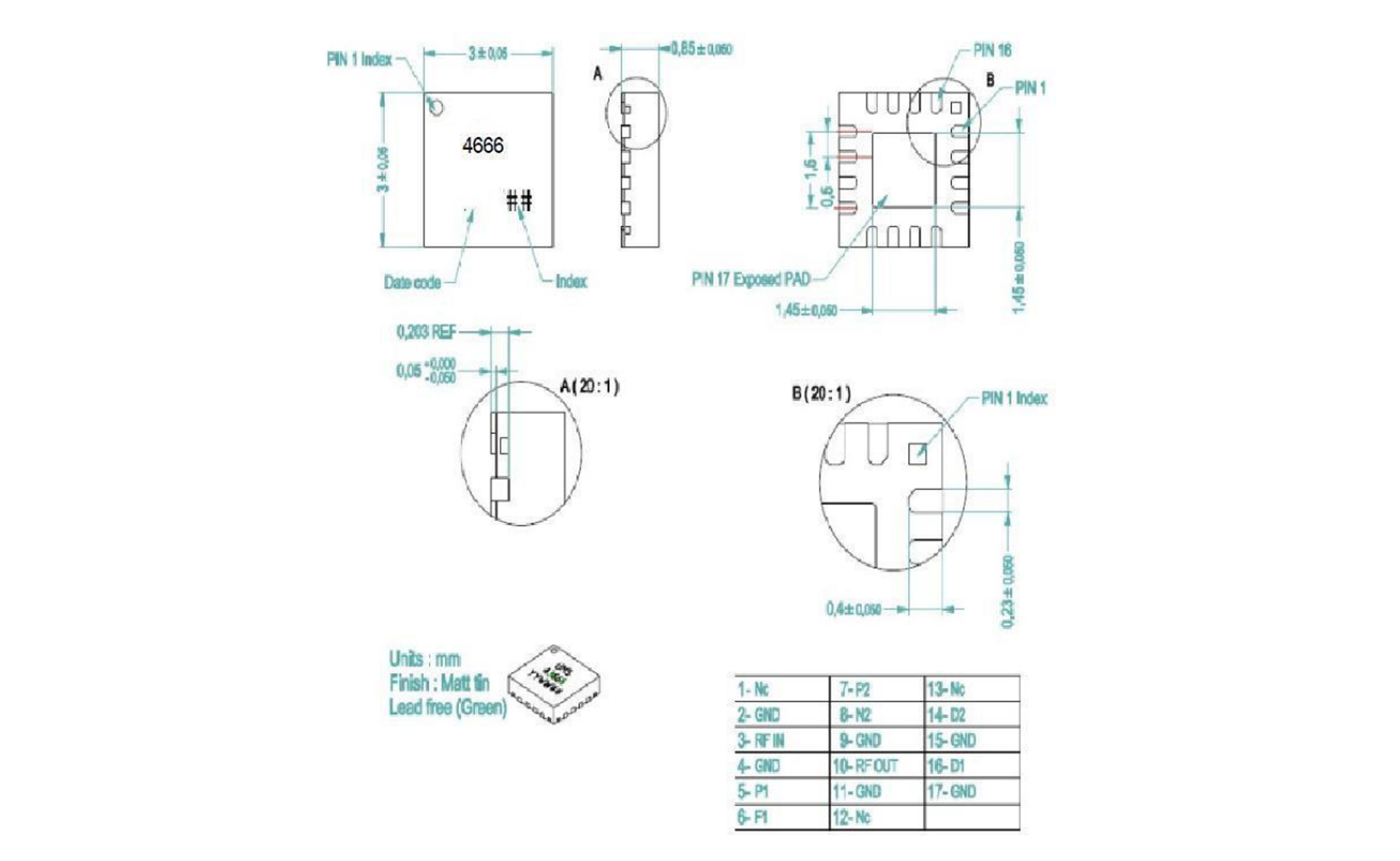
GA 4666
?

Category:


The GA 4666 is a two-stage self-biased wide band monolithic low noise amplifier.The circuit is manufactured with a standard pHEMT process: 0.25um gate length, viaholes through the substrate, air bridges and electron beam gate lithography. lt is supplied inlead-free package.
Main Features
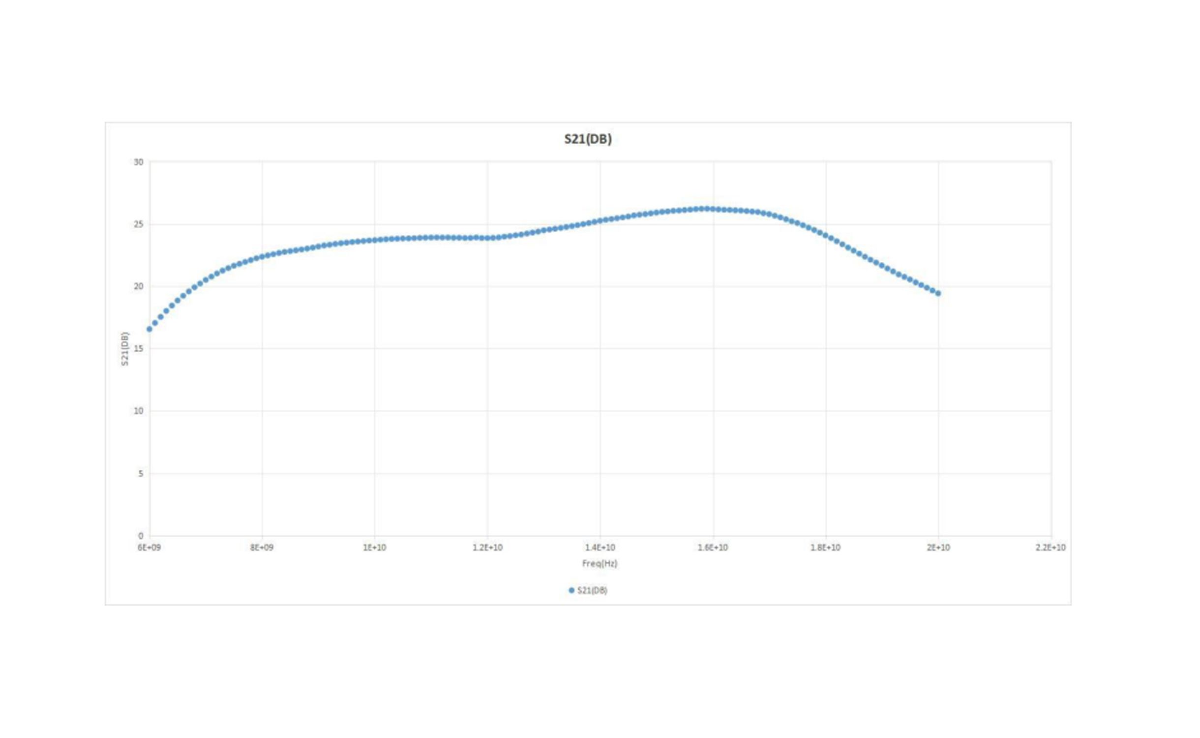
● Broadband performance 8-18GHz
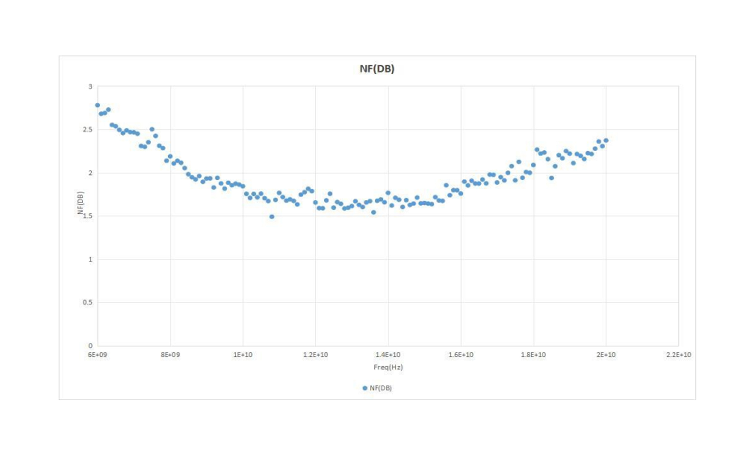
● 2.0dB noise figure
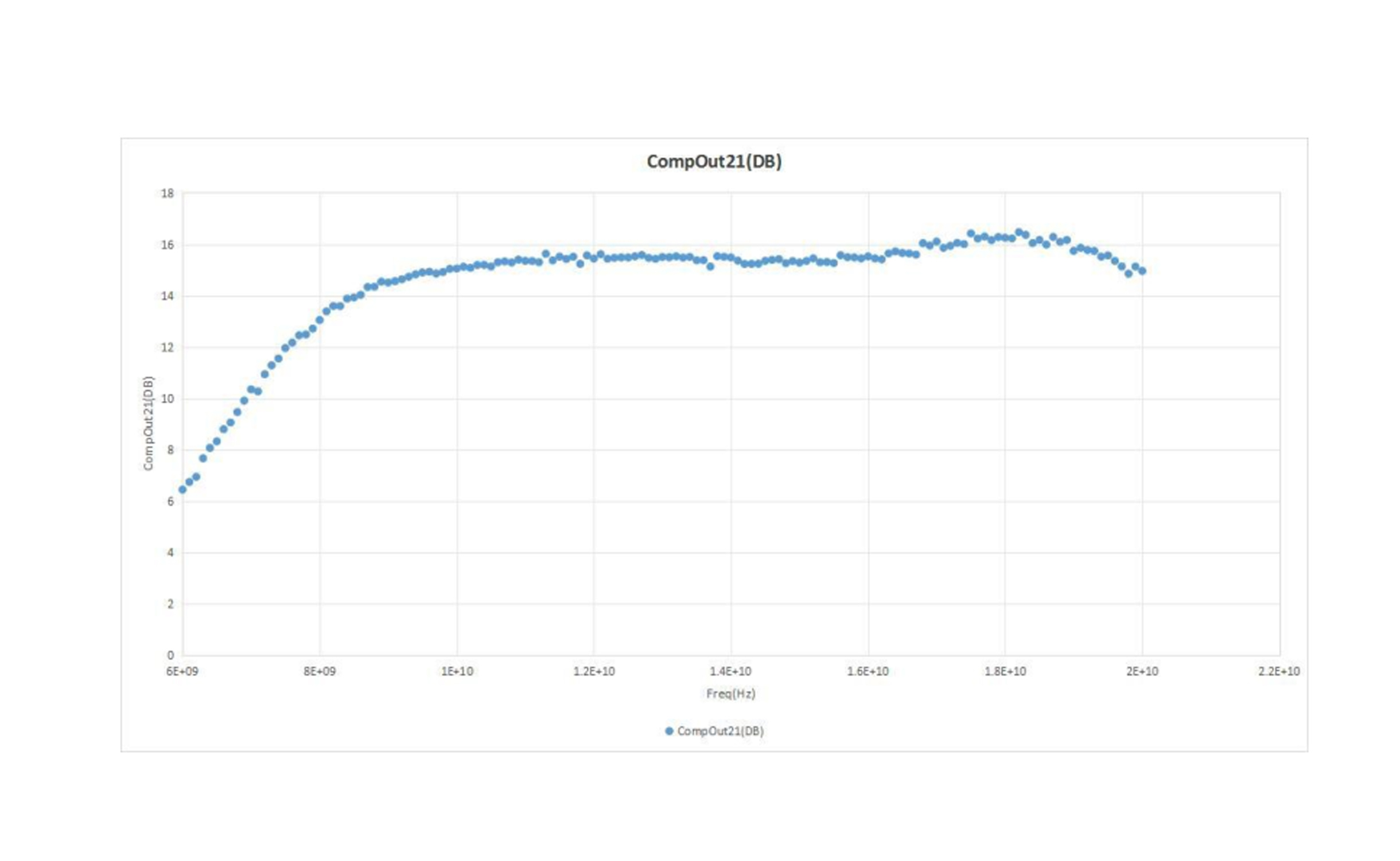
● 15dBm power at 1dB compression
● 23dB gain
● Low DC power consumption
● 16L-QFN3X3 SMD package
Main Electrical Characteristics
Tamb.=+25°C,Vd1=Vd2=+5V,P1& N2=GND
| Symbol | Parameter | Min | Typ | Max | Unit |
| Freg | Frequency range | 8 | 18 | GHz | |
| NF | Noise Figure | 1.8 | 2 | dB | |
| G | Gain | 21 | 22 | 23 | dB |
| IP3 | 3rd order intercept point | 26 | dBm | ||
| S11 | Input return loss (2) | -17.86 | -16 | dB | |
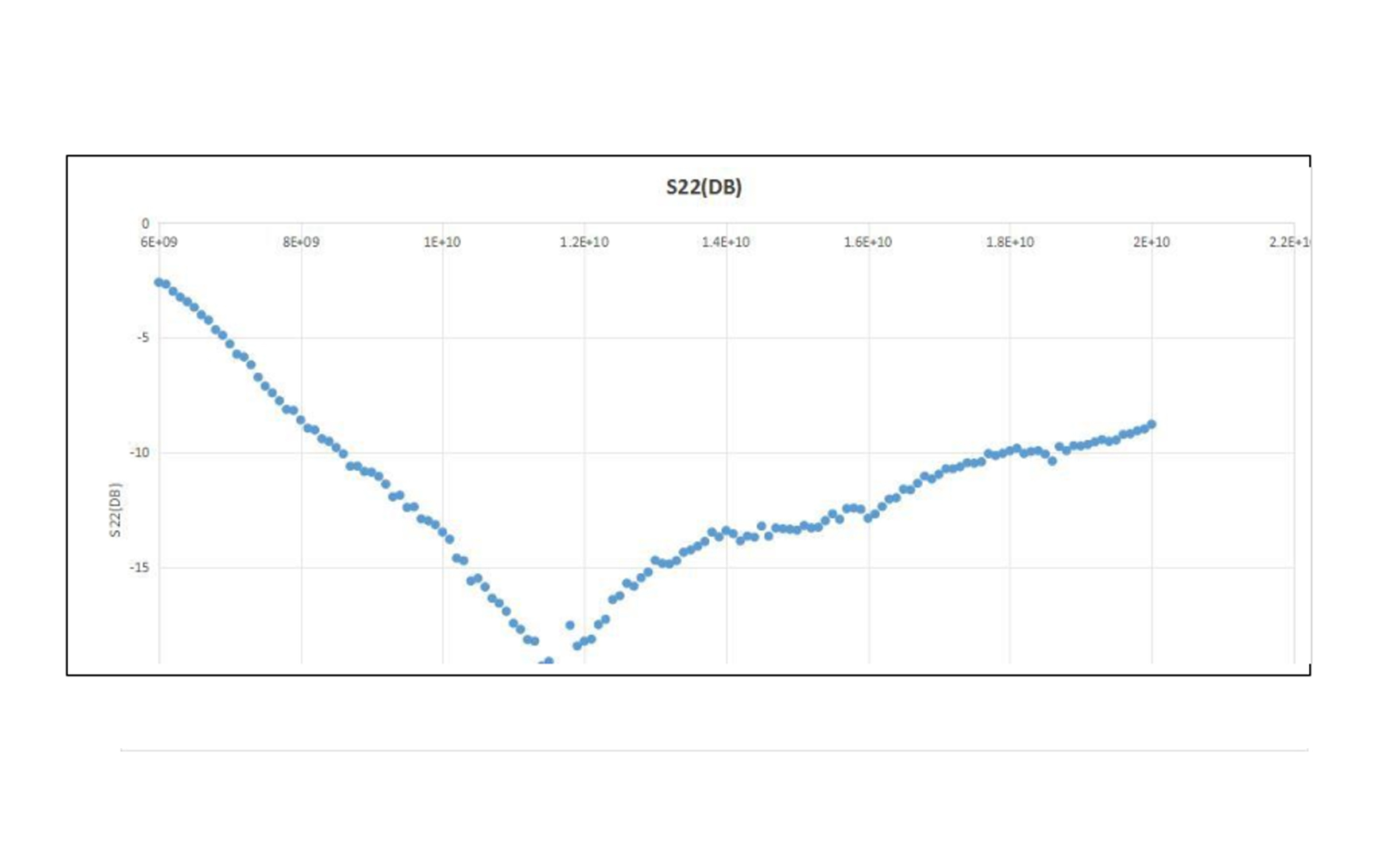
| S22 | Output return loss (2) | -16 | -12 | dB | |
| IP3 | 3rd order intercept point | 26 | dBm | ||
| P1dB | Output power at 1 dB gain comp (2)(3) | 13 | 15 | 16 | dBm |
| Vd1, 2 | Drain bias voltage | 6 | V | ||
| ld | Drain bias current | 40 | 55 | 70 | mA |
Absolute Maximum Ratings (1)
Tamb.= +25°C
| Symbol | Parameter | Values | Unit |
| Vd | Drain bias voltage | 5.5 | V |
| Pin | RF input power | 10 | dBm |
| Top | Operating temperature range | -40 to +85 | °C |
| Tj | Maximum Junction temperature (2) | 175 | °C |
(1) Operation of this device above anyone of these parameters may cause permanent damage.
(2)Thermal Resistance channel to ground paddle
Recommended Operating Range
| Symbol | Parameter | Values | Unit |
| Vd | Drain bias voltage | 4 to 5 | V |
| Pin | Maximum peak input power overdrive | 5 | dBm |
Temperature Range
| Ta | Operating temperature range | -40 to +95 | °C |
| Tstg | Storage temperature range | -55 to +150 | °C |
Gain vs.Frequency
NF vs. Frequency
P-1dB vs .Frequency
Output return loss vs. Frequency(S22)
Input return loss VS.Frequency (S11)

Previous
Next
Inquire Now
Note: Please leave your email address, our professionals will contact you as soon as possible!
Related Products