
Products
Related Posts
What is
GA777
?

Category:


Overview
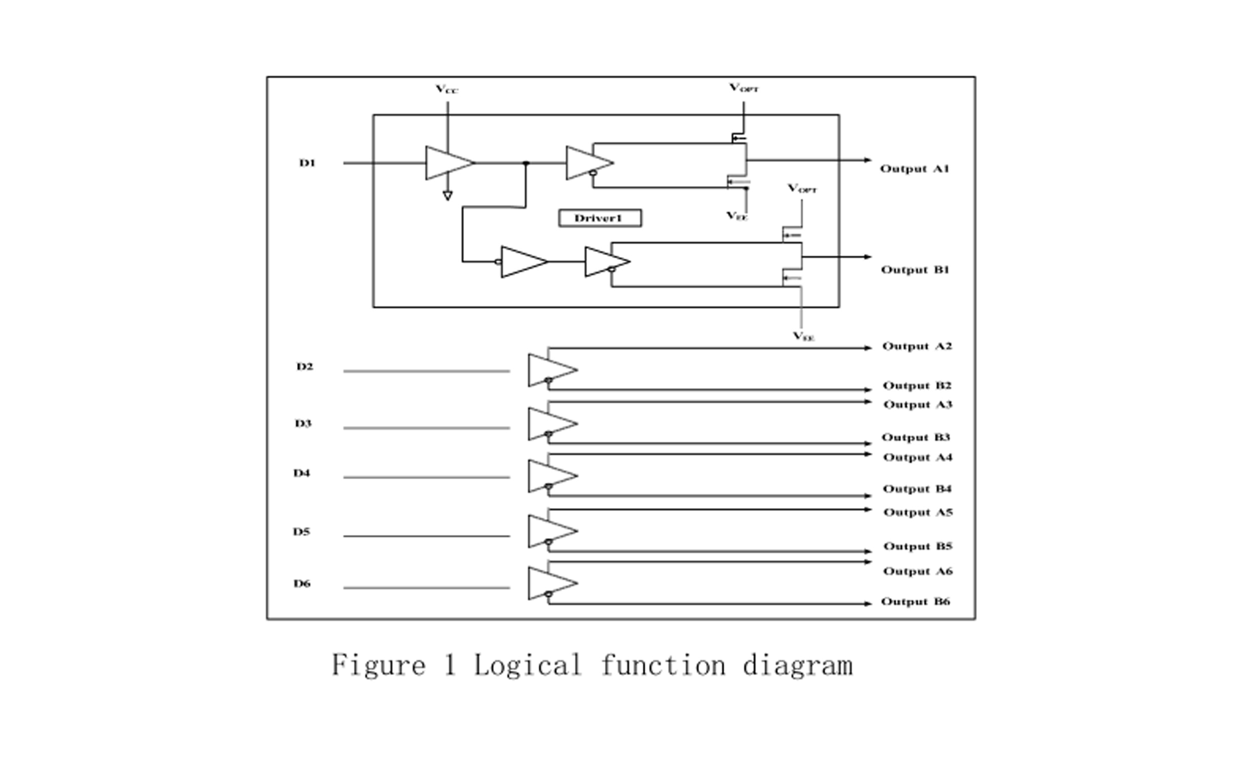
The main function of the GA777 beam control special circuit is to convert theinput parallel 6-bit data into 6 pairs
Technical specifications
2.1 Function description
The 6 bits of data entered are: Dl, D2, D3, D4, D5, D6.The output 12-bit differential signal is:$1+&S1-S6+&S6- where + is the inphase output and_is the inverse-phase output.VOPT corresponds to the differential output high level voltage value.
2.2 Principle description
The ASIC is composed of digital and analog parts. The digital part iscomposed of a series and transfer shift register, a buffer register, a multiplexswitch and other functional circuits. The analog part is composed of voltageconversion circuit and poweron reset circuit.
After the power on the circuit, the poweron reset module begins to work.the digital part of the register, clock, data for zeroing, about 10us end zeroing,the digital part of the circuit with the clock to achieve the data series and conversion,through the DARY signal control of the parallel data into the analog part of thecircuit, the output after driving amplification.
2.3 Logic function diagram
See Figure l for the logic function diagram.
2.4 Truth Table
The chip is divided into six output drivers, Each circuit works in a similarway, TTl level control signal input to the circuit is converted to produce gate controlvoltage required to control microwave switch and attenuator of gallium arsenide device. Inputlevel swing can be 0.8V~2.0V(VIL=0.8V, VIH=2.0V) when the circuit is working. Theoutput level is converted to the oupu level with a swing of -0. 5V~0V(VEE=-5.0V VOPT-0V)in typical applications. The true values are shown in Table 1.
Table l Truth table
| Six input signals | Six output signals |
| Dx | AX_DX,BX= DX |
| Where X=1~6 | |
2.5 Electrical parameters
The working environment is shown in Table 2
Table 2Work environment
| Recommended Working Conditions | Absolute maximum rating |
| Operating voltage vpp):4.5V~5.5V | 0perating voltage (VDD):7V |
| Working voltage(vEE): -5.5V~-4.5V | Operating voltage(VEE):-6V |
| Working ambient temperature(TA):-55°℃~125°C | / |
| Storage temperature:-65°C~150C | / |
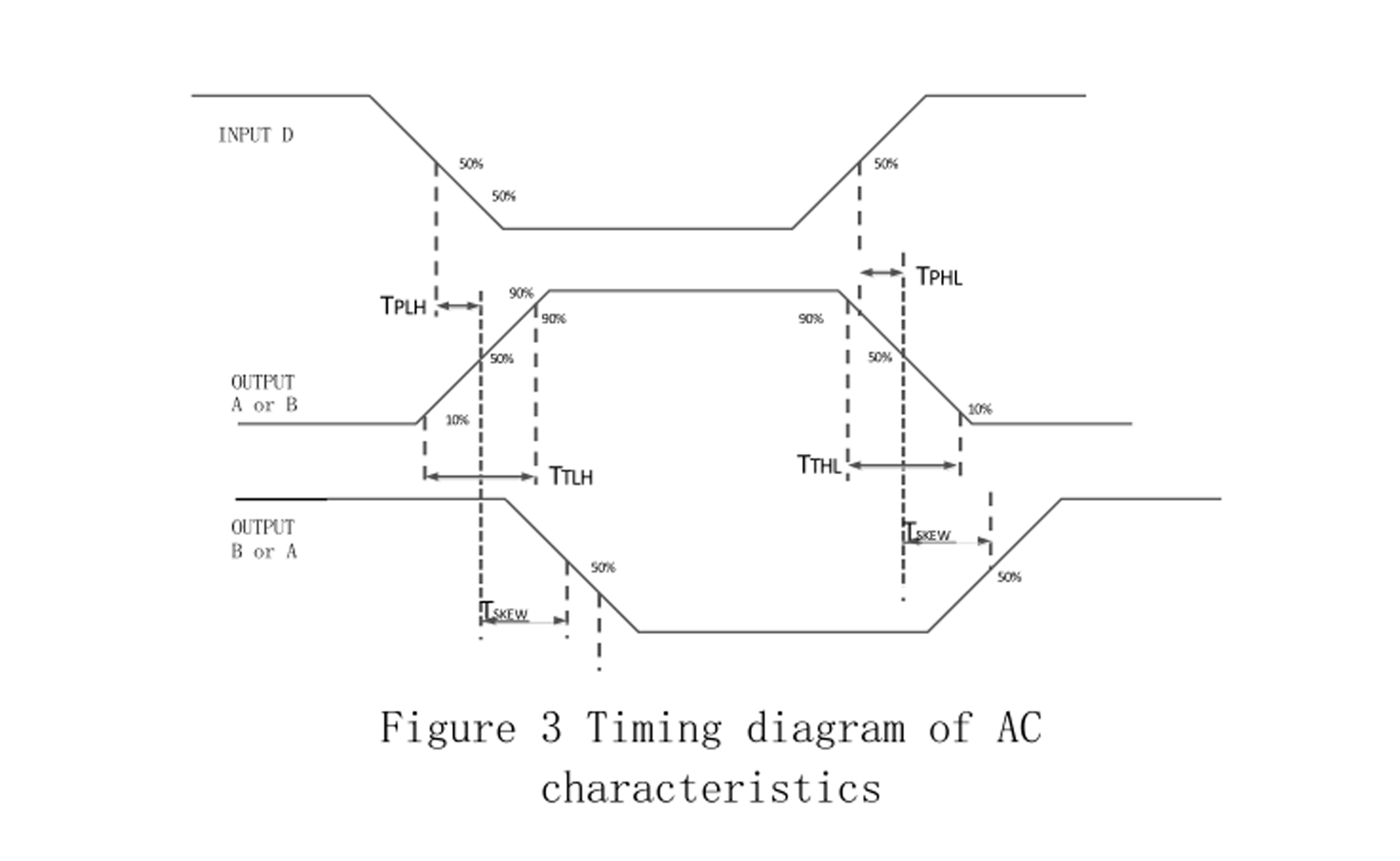
The parameters are shown in Table 3, and the timing diagram of ACcharacteristics is shown in Figure 3.
Table 3 Electrical parameters
| Characteristics | Symbols | ConditionsUnless otherwise specifiedVCC-5V vEE- -5V vGND-oV, VOPT=ov,TA=25°C | Limiting Value | Units | |
| Minimum | Maximum | ||||
| Static current(vcc) | Icc | 0utput no-load | - | 5 | MuA |
| Input signal high level threshold | VIH | - | 2.0 | V | |
| Input signal low threshold | VIL | 0.8 | - | V | |
| Input high level leakage current | IIH | Vcc=5.5V V1=5.5V | - | 1 | MuA |
| Input low-level leakage current | IIL | Vcc=5.5 VVI -0V | - | -1 | MuA |
| Differential drive output high level voltage | VOH | IOH=-1mA VEE=-5.0V | 0.2 | - | V |
| Differential drive output low-level voltage | VOL | IOL=-1mA VEE=-5.0V | 4.8 | V | |
| Dynamic Current(vcc) | IDD | Each input f= 10MHz at the sametime | - | 1 | mA |
| Dynamic Current (vEE) | IEE | When each input f=1MHzsimultaneously(no load) | - | 3 | mA |
| Note 1: All voltages are based on GND. GND=0V, the current is positive with the inletdevice outlet. Note 2:The equivalent value of output load in dynamic parameter test is CL-20pF |
|||||
Chip shape and PAD definition
3.1 Chip
GA777 chip layout is shown in Figure 4.
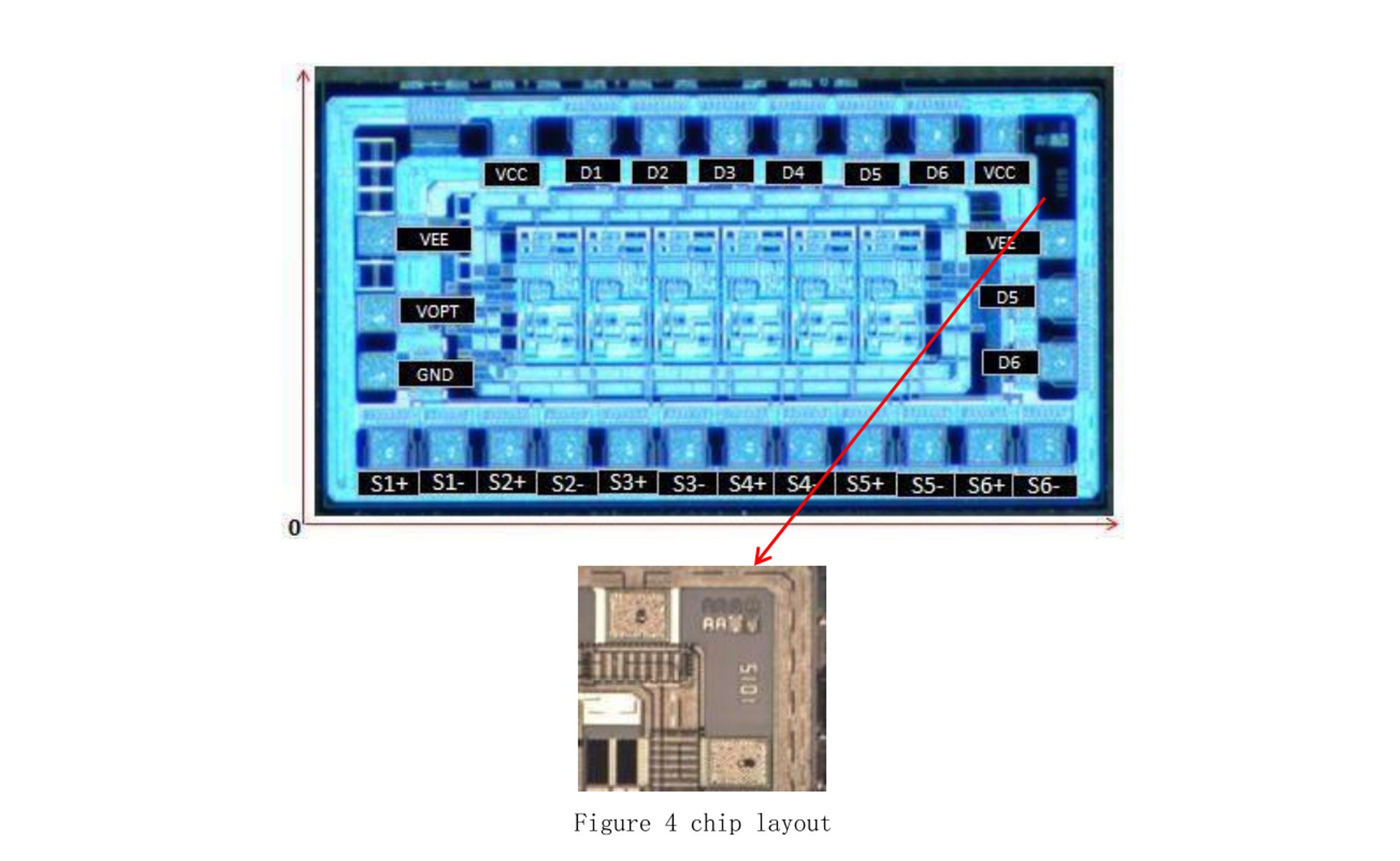
Chip size:2360umx1200umx400um(excluding the scribing slot);
xx(including the scribing slot).
PAD size :90 x90.
Chip is N type substrate, substrate potential vop or suspended.
3.2 PAD coordinates and instructions
GA777 PAD coordinates and descriptions are shown in Table 4.
Table 4 PAD coordinates and description(the origin of coordinates is the lowerleft point of the chip)
| Serial number | PAD name | Coordi nate X(u) | Coordi natey Y (um) | I/O | Features |
| 1 | Vcc | 566 | 1080 | P | +5V power supply |
| 2 | VEE | 151 | 785 | P | -5V power supply |
| 3 | VOPT | 151 | 558 | P | 0ptional output power supply |
| 4 | GND | 151 | 386 | P | referentially |
| 5 | S1+ | 181 | 157 | O | Same way output lst way |
| 6 | S1- | 365 | 157 | O | Reverse output route 1 |
| 7 | S2+ | 548 | 157 | O | Same way output 2nd way |
| 8 | S2- | 731 | 157 | O | Reverse output route 2 |
| 9 | S3+ | 914 | 157 | O | Same way output 3rd way |
| 10 | S3- | 1097 | 157 | O | Reverse output route 3 |
| 11 | S4+ | 1281 | 157 | O | Same direction output route 4 |
| 12 | S4- | 1464 | 157 | O | Reverse output route 4 |
| 13 | S5+ | 1647 | 157 | O | Same direction output route 5 |
| 14 | S5- | 1830 | 157 | O | Reverse output route 5 |
| 15 | S6+ | 2013 | 157 | O | Same direction output route 6 |
| 16 | S6- | 2197 | 157 | O | Reverse output route 6 |
| 17 | D6 | 2235 | 403 | I | Enter Route 6(alternate input port) |
| 18 | D5 | 2235 | 592 | I | Enter Route 5(alternate input port ) |
| 19 | VEE | 2235 | 767 | P | -5V power supply |
| 20 | Vcc | 2060 | 1080 | P | +5V power supply |
| 21 | D6 | 1860 | 1080 | I | Enter route 6 |
| 22 | D5 | 1650 | 1080 | I | Enter route 5 |
| 23 | D4 | 1440 | 1080 | I | Enter route 4 |
| 24 | D3 | 1230 | 1080 | I | Enter route 3 |
| 25 | D2 | 1020 | 1080 | I | Enter route 2 |
| 26 | D1 | 810 | 1080 | I | Enter route 1 |
Precautions
4.1 Configuration requirements
vDD and VEE need to be configured with 0.luF filter capacitor to GN.
4.2 Packaging Requirements
The chip packaging shall comply with the provisions of GJB 2835-1997, and bepacked in a special anti-static material box and vacuum-packed with anti-staticaluminum film, The outer packaging shall be in a carton. The chip packing box shall beaccompanied with the product certificate.
4.3 Storage requirements
The chip should be packed in the corresponding packaging container providedby our company, and the packaging container should be stored in therelative humidity ofThe drying box or drying tower in the range of 20%RHto 75%RH, and keep thetemperature range of 5'C to 30C, The effective storage period of the chipmeeting the above conditions is 3 years. If more than the effective storageperiod,according to user requirements for reinspection,reinspection can continueto supply.
4.4 Transportation requirements
The product should be protected from rain and snow and mechanical impactduring transportation.
4.5 Anti-static requirements
Devices in accordance with this specification are electrostatic sensitive devices, and antistatic measures should be taken throughout storage, transportation and use.
Previous
Next
Inquire Now
Note: Please leave your email address, our professionals will contact you as soon as possible!
Related Products