Products

What is

Low Noise Amplifier & Switch

?

+
We has volume-produced high-precision analog-to-digital converters (ADC), digital-to-analog converters (DAC), and clock driver chips, all of which have achieved industry-leading specifications. Additionally, these products are capable of seamless pin-to-pin replacements with other advanced chip products. Our ADC and DAC products are renowned for their exceptional accuracy, low power consumption, and high speed, meeting the diverse application requirements ranging from industrial automation to communication systems, and medical devices. These products are meticulously designed to ensure stable and reliable performance under various harsh environments. Clock driver chips represent another core technology of ours, providing precise timing control for high-speed data transmission and being indispensable components in many high-performance computing and communication systems. Our clock driver chips feature low jitter, high-frequency stability, and excellent phase noise performance, ensuring system synchronicity and overall functionality. The volume-produced MCU chips are celebrated for their high performance, low power consumption, and extensive integrated functionalities, catering to a wide range of applications from automotive, smart home devices to industrial automation, and IoT devices. These products are carefully engineered to deliver stable and reliable performance under stringent environmental conditions.
div[class^="e_richText"] .table table.buyao td {border:none !important;}
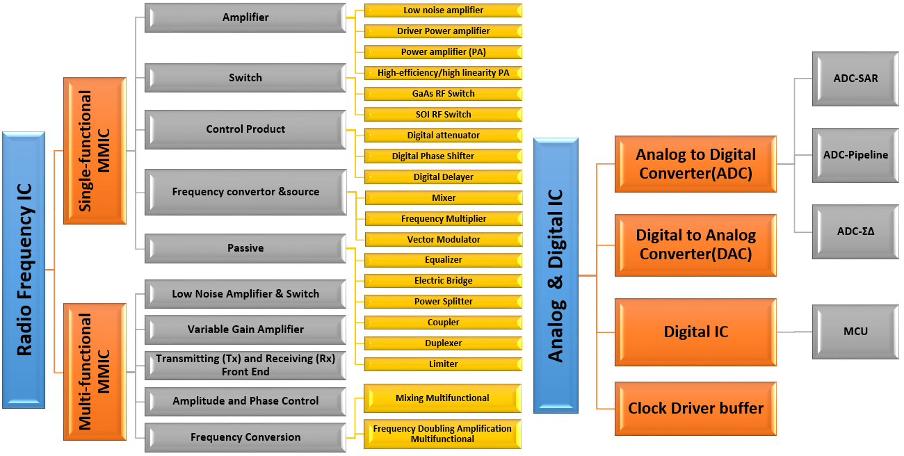
Roadmap of ICs
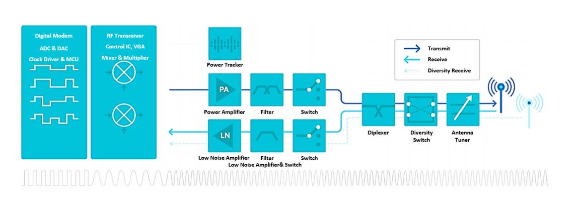
Application of ICs in the communication system
Low Noise Amplifier & Switch
Product to Replace Frequency (GHz) TX Insertion loss
(dB)
switching speed(ns) RX P-1
 (dBm)
RX OIP3 (dBm) RX Noise figure
(dB)
RX Gain
(dB)
Isolation
(dB)
TX Power handling(dBm) Size
(mm)
GAF0201 ARRF5549 1.88~2.7 0.4 761 17/16 31/31 1.0/1.1 37/17.5 38 43 6.2 × 6.2 LGA 
GAF0202 ADRF5545A 2.3-5 0.5 260 18/17 28/23 1.4/1.4 30/17.7 55 40 6.2 × 6.2 LGA 
GAF0203 - 3.3~4.2 0.4 754 16/15 27.5/17.6 1.1/1.15 36/17.5 38 43 6.2 × 6.2 LGA 
GAF0204 ADRF5545 2.3-5 0.5 260 18/17 28/23 1.4/1.4 30/17.7 55 39 6.2 × 6.2 LGA 
GAF0205   2.3-5 0.5 260 19/17 28/28 1.2/1.2 32/16 55 40 6.2 × 6.2 LGA 
GAF0206 - 2.4-2.6 0.45 280 18.3/14.5 29/22 1.35/1.1 28.5/17 55 38 6×6 LGA 
GAF0207 - 3.3-4.2 0.4 754 16/15 27.5/17.6 1.1/1.15 36/17.5 38 43 6.2 × 6.2 LGA 
GAF0208 - 3.4-3.8 0.5 280 18/17.3 28/23 1.35/1.15 30.1/16.6 55 38 6×6 LGA 
GAF0209 - 4.4-4.99 0.55 280 17/16 29/25 1.4/1.3 27/16 55 38 6×6 LGA 


Inquire Now

Note: Please leave your email address, our professionals will contact you as soon as possible!

Related Products

GA9354C


The GA29F040 is a 4-mega bit Flash memory organized as 512K bytes of 8 bits. Flash memories offer the most cost-effective and reliable read/write non volatile random access memory. The GA29F040 is packaged in 32-pin PLCC, TSOP, PDIP. It is designed to be reprogrammed and erased in system or in standard EPROM programmers. The standard GA29F040 offers access time as fast as 55ns, allowing operation of high-speed microprocessors without wait states. To eliminate bus contention, the GA29F040 has separate chip enable (CE#) and output enable (OE#) controls. Flash memories augment EPROM functionality with incircuit electrical erasure and programming. The GA29F040 uses a command register to manage this functionality. The command register allows for 100% TTL level control inputs and fixed power supply levels during erase and programming, while maintaining maximum EPROM compatibility. Flash technology reliably stores memory con- tents even after 100,000 erase and program cycles. The cell is designed to optimize the erase and program mechanisms. In addition, the combi- nation of advanced tunnel oxide processing and low internal electric fields for erase and programming operations produces reliable cycling. The GA29F040 uses a 5.0V 10% VCC supply to per- form the High Reliability Erase and auto Program/ Erase algorithms. The highest degree of latch-up protection is achieved with proprietary non-epi process. Latch-up protection is proved for stresses up to 100 milliamps on address and data pin from -1V to VCC + 1V.

GA29F040


The GA29F040 is a 4-mega bit Flash memory organized as 512K bytes of 8 bits. Flash memories offer the most cost-effective and reliable read/write non volatile random access memory. The GA29F040 is packaged in 32-pin PLCC, TSOP, PDIP. It is designed to be reprogrammed and erased in system or in standard EPROM programmers. The standard GA29F040 offers access time as fast as 55ns, allowing operation of high-speed microprocessors without wait states. To eliminate bus contention, the GA29F040 has separate chip enable (CE#) and output enable (OE#) controls. Flash memories augment EPROM functionality with incircuit electrical erasure and programming. The GA29F040 uses a command register to manage this functionality. The command register allows for 100% TTL level control inputs and fixed power supply levels during erase and programming, while maintaining maximum EPROM compatibility. Flash technology reliably stores memory con- tents even after 100,000 erase and program cycles. The cell is designed to optimize the erase and program mechanisms. In addition, the combi- nation of advanced tunnel oxide processing and low internal electric fields for erase and programming operations produces reliable cycling. The GA29F040 uses a 5.0V 10% VCC supply to per- form the High Reliability Erase and auto Program/ Erase algorithms. The highest degree of latch-up protection is achieved with proprietary non-epi process. Latch-up protection is proved for stresses up to 100 milliamps on address and data pin from -1V to VCC + 1V.

Business license

Address: Beijing Tongzhou District Xiji Town, Wanganyuan Innovation Center 1-198