
Products
Related Posts
What is
Passive
?


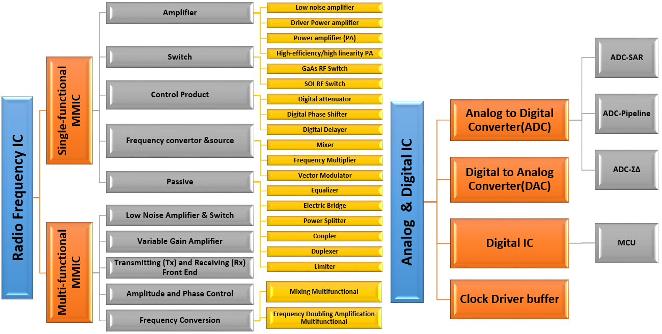
Roadmap of IC
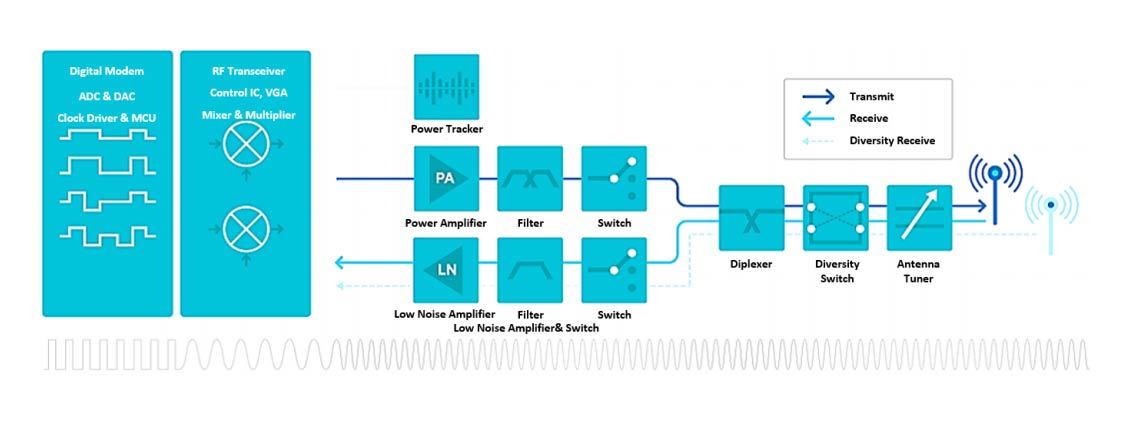
Application of ICs in the communication system
Equalizer
| Product | Frequency (GHz) | Equilibrium Quantity(dB) | Insertion loss(dB) | Input VSWR | Output VSWR | Size (mm) |
| GAK0101 | 0.01-1.2 | 10 | 2.4@1.2GHz | 1.2 | 1.2 | 1.2×1.2×0.1 |
| GAK0102 | 6-18 | 4 | 0.55@18GHz | 1.2 | 1.2 | 0.74×0.8×0.1 |
| GAK0103 | 2-18 | 5 | 0.65@18GHz | 1.1 | 1.1 | 0.75×1.2×0.1 |
| GAK0104 | 2-6 | 6 | 0.86@6GHz | 1.3 | 1.3 | 0.74×0.945×0.1 |
| GAK0105 | 6-18 | 6 | 0.93@18GHz | 1.3 | 1.3 | 0.74×0.8×0.1 |
| GAK0106 | 2-18 | 2 | 0.65@18GHz | 1.2 | 1.2 | 0.75×1.2×0.1 |
| GAK0107 | 2-18 | 8 | 0.7@18GHz | 1.1 | 1.1 | 0.75×1.2×0.1 |
| GAK0108 | 0.8-8.5 | 9 | 2.7@8.5GHz | 1.2 | 1.2 | 0.92×0.8×0.1 |
| GAK0109 | 0.8-2.7 | -1.4@0.8-1.6GHz, 5.8@1.6-2.7GHz | 1.2@2.7GHz | 1.3 | 1.3 | 1.2×1.5×0.1 |
| GAK0110 | 26-40 | 4 | 2.2@40GHz | 1.3 | 1.3 | 0.74×0.5×0.1 |
| GAK0111 | 2-6 | 2 | 0.26@6GHz | 1.2 | 1.2 | 0.74×0.945×0.1 |
| GAK0112 | 6-18 | 2 | 0.63@18GHz | 1.2 | 1.2 | 0.74×0.8×0.1 |
| GAK0113 | 8-12 | 3 | 0.82@12GHz | 1.3 | 1.3 | 0.74×0.8×0.1 |
| GAK0114 | 0.5-20 | 14 | 1.1@20GHz | 1.3 | 1.3 | 0.85×0.8×0.1 |
| GAK0115 | 2-6 | 4 | 1@6GHz | 1.1 | 1.1 | 1×1.3×0.1 |
| GAK0116 | 18-40 | 6 | 2.2@40GHz | 1.4 | 1.4 | 0.74×0.5×0.1 |
| GAK0117 | 0.5-20 | 16 | 1.4@20GHz | 1.2 | 1.2 | 0.85×0.8×0.1 |
| GAK0118 | 2-18 | 3 | 0.54@18GHz | 1.2 | 1.2 | 0.75×1.2×0.1 |
| GAK0119 | 0.8-2.7 | 4 | 0.6@2.7GHz | 1.1 | 1.1 | 1.2×1.5×0.1 |
| GAK0120 | 2-18 | 7 | 0.7@18GHz | 1.1 | 1.1 | 0.75×1.2×0.1 |
| GAK0121 | 26-40 | 10 | 2.6@40GHz | 1.3 | 1.3 | 0.74×0.5×0.1 |
| GAK0122 | 2-6 | 4 | 0.58@6GHz | 1.2 | 1.2 | 0.74×0.945×0.1 |
| GAK0123 | 2-6 | 2 | 1@6GHz | 1.1 | 1.1 | 1×1.3×0.1 |
| GAK0124 | 0.5-20 | 12 | 0.9@20GHz | 1.3 | 1.3 | 0.85×0.8×0.1 |
| GAK0125 | 18-40 | 3 | 2.2@40GHz | 1.5 | 1.5 | 0.74×0.5×0.1 |
| GAK0126 | 6-18 | 4 | 0.6@18GHz | 1.2 | 1.2 | 1×1.3×0.1 |
| GAK0127 | 2-6 | 2 | 0.25@6GHz | 1.2 | 1.2 | 3×3×0.1 |
| GAK0128 | 2-6 | 6 | 2.4@6GHz | 1.2 | 1.2 | 1×1.3×0.1 |
| GAK0129 | 2-18 | 6 | 0.72@18GHz | 1.1 | 1.1 | 0.75×1.2×0.1 |
| GAK0130 | 18-40 | 10 | 3.2@40GHz | 1.3 | 1.3 | 0.74×0.5×0.1 |
| GAK0131 | 6-18 | 8 | 1.26@18GHz | 1.4 | 1.4 | 0.74×0.8×0.1 |
| GAK0132 | 6-18 | 10 | 1.65@18GHz | 1.4 | 1.4 | 0.74×0.8×0.1 |
| GAK0133 | 6-18 | 10 | 1.8@18GHz | 1.3 | 1.3 | 1×1.3×0.1 |
| GAK0134 | 6-18 | 5 | 1.4@18GHz | 1.3 | 1.3 | 1×1.3×0.1 |
| GAK0135 | 2-18 | 4 | 0.53@18GHz | 1.1 | 1.1 | 0.75×1.2×0.1 |
| GAK0136 | 2.5-12 | 4/6/8 | 0.8@12GHz | 1.4 | 1.4 | 2×0.75×0.1 |
| GAK0137 | 26-40 | 6 | 1.7@40GHz | 1.3 | 1.3 | 0.74×0.5×0.1 |
Electric Bridge
| Product | Frequency (GHz) | Insertion loss(dB) | Isolation(dB) | Input VSWR | Output VSWR | Size (mm |
| GAM0101 | 6-18 | 1 | 18 | 1.3 | 1.3 | 1.1×3.9×0.1 |
Power Splitter
| Product | Frequency (GHz) | Insertion loss(dB) | Isolation(dB) | Input VSWR | Output VSWR | Size (mm) |
| GAL0101 | 0.8-2 | 1.2 | 13 | 1.1 | 1.3 | 1.5×3.7×0.1 |
| GAL0102 | 6-18 | 1.1 | 13 | 1.6 | 1.4 | 1.5×1.5×0.1 |
| GAL0103 | 6-18 | 1 | 15 | 1.6 | 1.6 | 1×0.8×0.1 |
| GAL0104 | 6.8-7.2 | 1.6 | 20 | 1.3 | 1.3 | 3.0×3.0×0.9 |
| GAL0105 | 6.8-7.2 | 3.2 | 21 | 1.4 | 1.3 | 3.0×3.0×0.9 |
| GAL0106 | 24-40 | 1.3 | 15 | 1.6 | 1.5 | 1.2×3.2×0.1 |
| GAL0107 | 0.8-6 | 1 | 15.5 | 1.4 | 1.4 | 2.2×3.9×0.1 |
| GAL0108 | 2-6 | 0.8 | 13 | 1.6 | 1.4 | 1.5×1.5×0.1 |
| GAL0109 | 18-26.5 | 0.8 | 20 | 1.4 | 1.4 | 1.2×3.9×0.1 |
| GAL0110 | 1-3 | 1 | 15 | 1.4 | 1.4 | 1.4×1.12×0.1 |
| GAL0111 | 1-18 | 1.8 | 13 | 1.4 | 1.2 | 2.6×2.2×0.1 |
| GAL0112 | 4.6-4.72 | 1.2 | 36 | 1.4 | 1.2 | 3×3×0.9 |
| GAL0113 | 1.6-3.3 | 0.8 | 27 | 1.3 | 1.1 | 3.0×3.0×0.9 |
Coupler
| Product | Frequency (GHz) | Insertion loss(dB) | Coupling(dB) | coupling flatness(dB) | VSWR | Size (mm) |
| GAN0101 | 2-6 | 0.5 | `15 | 3 | 1.1 | 4.2×1.75×0.1 |
| GAN0102 | 6-18 | 0.3 | 20 | 3 | 1.2 | 2.0×1.1×0.1 |
| GAN0103 | 2-6 | 0.2 | 20 | 3 | 1.1 | 3.2×1.4×0.1 |
| GAN0104 | 2-6 | 0.4 | 15 | 3 | 1.1 | 3.2×1.4×0.1 |
| GAN0105 | 6-18 | 1 | 20 | 4 | 1.2 | 2.8×3.2×0.1 |
Duplexer
|
Product
|
Frequency (GHz)
|
Insertion loss(dB)
|
Isolation(dB)
|
Input VSWR
|
Output VSWR
|
Size (mm)
|
| GAO0101 | 19.6-21.2 | 1.0@19.6-21.2GHz | 45 | 1.3 | 1.2 | 0.945×2×0.1 |
| GAO0102 | 29.4-31 | 1.3@29.4-31GHz |
Limiter
| Product | Frequency (GHz) | Insertion loss(dB) | Output VSWR | Power endurance (W) | Input VSWR | Size (mm) |
| GAP0101 | DC-18 | 0.5 | 1.3 | 5 | 1.3 | 1.23×0.66×0.1 |
Previous
Next
Inquire Now
Note: Please leave your email address, our professionals will contact you as soon as possible!
Related Products