
Products
Related Posts
What is
Clock Driver buffer
?


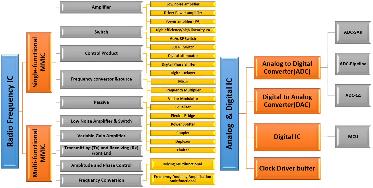
Roadmap of ICs
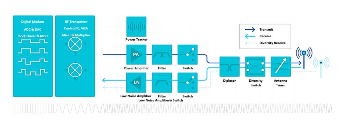
Application of ICs in the communication system:
Clock Driver buffer
| Product | P2P to Replace | Characteristic | Outp ut Chan nel | Freque ncy (MHz) | Tempe rature (℃) | Addit ional Jitter (fs) | RMS Jitter (ps) | C2C Jitter (ps)Skew (ps) | Skew (ps) | Working Current (mA) | Output Voltage (V) | Working Voltage (V) | Package |
| GAD3320 | CY2305 | Zero | 5 | 10~200 | - 40~110 | N.A. | 3 | 60 | <50 | 15 | 3.3 | 3.3 | SOIC-8 |
| GAD3346 | 8L30110 cdclvc1310 Au5410 LMK00101 PI6C49X0210 8L30110 8L30210 PI6C49X0210- A | HCSL, LVCMOS, LVDS, LVPECL, SSTL, XTAL Input LVCMOS / LVTTL Output | 10 | 10~250 | - 40~110 | 45 | N.A. | N.A. | <60 | 1 | 1.5, 1.8, 2.5, 2.8 | 3.3, 2.5 | QFN32 |
| GAD3328 | 8L3010 | HCSL, LVCMOS, LVDS, LVPECL, SSTL, XTAL Input LVCMOS / LVTTL Output | 10 | 10~250 | - 40~110 | 45 | N.A. | N.A. | <60 | 1 | 1.5, 1.8, 2.5, 2.8 | 3.3, 2.5 | QFN32 |
| GAD3332 | CDCLVC1110 5PB1110 | HCSL, LVCMOS, LVDS, LVPECL, SSTL, XTAL Input LVCMOS / LVTTL Output | 10 | 10~250 | - 40~110 | 45 | N.A. | N.A. | <60 | 1 | 1.5, 1.8, 2.5, 2.8 | 3.3, 2.5 | QFN32 |
| GAD3344 | 74FCT3807S | HCSL, LVCMOS, LVDS, LVPECL, SSTL, XTAL Input;LVCMOS / LVTTL Output | 10 | 10~250 | - 40~110 | 45 | N.A. | N.A. | <60 | 1 | 1.5, 1.8, 2.5, 2.8 | 3.3, 2.5 | QFN32 |
| GAD3338 | CY2309CY2309 | HCSL, LVCMOS, LVDS, LVPECL, SSTL, XTAL Input LVCMOS / LVTTL Output | 9 | 10~250 | - 40~110 | 45 | N.A. | N.A. | <60 | 1 | 1.5, 1.8, 2.5, 2.8 | 3.3, 2.5 | QFN32 |
| GAD3340 | CDCLVC1108 LMK1C1108 5PB1108 | HCSL, LVCMOS, LVDS, LVPECL, SSTL, XTAL Input;LVCMOS / LVTTL Output | 8 | 10~250 | - 40~110 | 45 | N.A. | N.A. | <60 | 1 | 1.5, 1.8, 2.5, 2.8 | 3.3, 2.5 | QFN32 |
| GAD3342 | ICS552-02 ICS552-02S | HCSL, LVCMOS, LVDS, LVPECL, SSTL, XTAL Input;LVCMOS / LVTTL Output | 8 | 10~250 | - 40~110 | 45 | N.A. | N.A. | <60 | 1 | 1.5, 1.8, 2.5, 2.8 | 3.3, 2.5 | QFN32 |
| GAD3336 | ICS552A-01 | HCSL, LVCMOS, LVDS, LVPECL, SSTL, XTAL Input LVCMOS / LVTTL Output | 8 | 10~250 | - 40~110 | 45 | N.A. | N.A. | <60 | 1 | 1.5, 1.8, 2.5, 2.8 | 3.3, 2.5 | QFN32 |
| GAD3324 | PI6C49X0208 | HCSL, LVCMOS, LVDS, LVPECL, SSTL, XTAL Input LVCMOS / LVTTL Output | 8 | 10~250 | - 40~110 | 45 | N.A. | N.A. | <60 | 1 | 1.5, 1.8, 2.5, 2.8 | 3.3, 2.5 | QFN32 |
| GAD3360 | CDCLVC1106 LMK1C1106 5PB1106 | HCSL, LVCMOS, LVDS, LVPECL, SSTL, XTAL Input LVCMOS / LVTTL Output | 6 | 10~250 | - 40~110 | 45 | N.A. | N.A. | <60 | 1 | 1.5, 1.8, 2.5, 2.8 | 3.3, 2.5 | QFN32 |
| GAD3364 | PI6C49X0206 | HCSL, LVCMOS, LVDS, LVPECL, SSTL, XTAL Input LVCMOS / LVTTL Output | 6 | 10~250 | - 40~110 | 45 | N.A. | N.A. | <60 | 1 | 1.5, 1.8, 2.5, 2.8 | 3.3, 2.5 | QFN32 |
| GAD3380 | PI6C49X0204 PI6C49CB04 PI6C49CB04C ICS551 ICS551S ICS621 ICS621S ICS651 ICS651S | HCSL, LVCMOS, LVDS, LVPECL, SSTL, XTAL Input LVCMOS / LVTTL Output | 4 | 10~250 | - 40~110 | 45 | N.A. | N.A. | <60 | 1 | 1.5, 1.8, 2.5, 2.8 | 3.3, 2.5 | QFN32 |
| GAD3372 | PI6CV304 PI6CV2304 | HCSL, LVCMOS, LVDS, LVPECL, SSTL, XTAL Input LVCMOS / LVTTL Output | 4 | 10~250 | - 40~110 | 45 | N.A. | N.A. | <60 | 1 | 1.5, 1.8, 2.5, 2.8 | 3.3, 2.5 | QFN32 |
| GAD3376 | ICS524S | HCSL, LVCMOS, LVDS, LVPECL, SSTL, XTAL Input;LVCMOS / LVTTL Output | 4 | 10~250 | - 40~110 | 45 | N.A. | N.A. | <60 | 1 | 1.5, 1.8, 2.5, 2.8 | 3.3, 2.5 | QFN32 |
| GAD3404 | ICS553S 5T30553 | HCSL, LVCMOS, LVDS, LVPECL, SSTL, XTAL Input;LVCMOS / LVTTL Output | 4 | 10~250 | - 40~110 | 45 | N.A. | N.A. | <60 | 1 | 1.5, 1.8, 2.5, 2.8 | 3.3, 2.5 | QFN32 |
| GAD3378 | CDCLVC1104 LMK1C1104 5PB11104 | HCSL, LVCMOS, LVDS, LVPECL, SSTL, XTAL Input LVCMOS / LVTTL Output | 4 | 10~250 | - 40~110 | 45 | N.A. | N.A. | <60 | 1 | 1.5, 1.8, 2.5, 2.8 | 3.3, 2.5 | QFN32 |
| GAD3379 | PI6C49X0202 PI6C49CB02 | HCSL, LVCMOS, LVDS, LVPECL, SSTL, XTAL Input;LVCMOS / LVTTL Output | 2 | 10~250 | - 40~110 | 45 | N.A. | N.A. | <60 | 1 | 1.5, 1.8, 2.5, 2.8 | 3.3, 2.5 | QFN32 |
| GAD3368 | CDCLVC1102 LMK1C1102 5PB1102 | HCSL, LVCMOS, LVDS, LVPECL, SSTL, XTAL Input LVCMOS / LVTTL Output | 2 | 10~250 | - 40~110 | 45 | N.A. | N.A. | <60 | 1 | 1.5, 1.8, 2.5, 2.8 | 3.3, 2.5 | QFN32 |
| GAD3396 | Si53156 | PCIE GEN1/2/3/4/5 ,SATA | 6 | 100~30 0 | -40~85 | <100 | N.A. | N.A. | <50 | 40 | 3.3 | 3.3, 2.5 | QFN32 |
| GAD3400 | Si53302 | Diff:LVPECL, LVDS, HCSL Single:CMOS, SSTL, HSTL | 10 Diff 20 Single | 5-800 | -40~85 | <100 | N.A. | N.A. | <50 | 2 | 1.5, 2.5, 3.3 | 3.3, 2.5, 1.8 | QFN44 |
| GAD3377 | Si53302 | Diff:LVPECL, LVDS, HCSL Single:CMOS, SSTL, HSTL | 10 Diff 20 Single | 5-800 | -40~85 | <100 | N.A. | N.A. | <50 | 2 | 1.5, 2.5, 3.3 | 3.3, 2.5, 1.8 | QFN44 |
Previous
Next
Inquire Now
Note: Please leave your email address, our professionals will contact you as soon as possible!
Related Products