
Products
Related Posts
What is
GPE9354
?

Category:


Product Specification
SPDT High Power
UltraCMOS™ RF Switch
Rad hard for Space Applications
Features
• Single 3-volt power supply
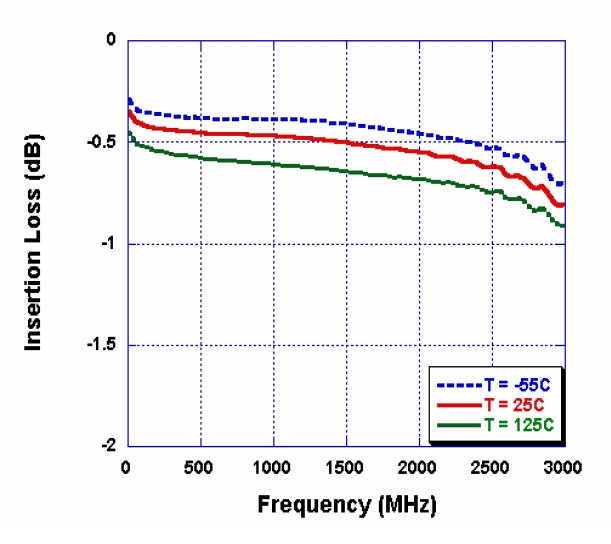
• Low insertion loss: 0.55 dB at 2000 MHz
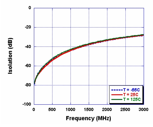
• High isolation of 30 dB at 2000 MHz
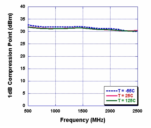
• Typical input 1 dB compression point of
+ 31 dBm
• 100 Krad total dose
• Single-pin CMOS or TTL logic control
• Low cost
| Figure 1. Functional Schematic Diagram | Figure 2. Package Type 8-lead CSOIC |
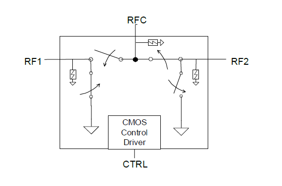 |  |
Table 1. A/C Electrical Specifications -55 °C to +125 °C, VDD = 3.0 V (ZS = ZL = 50 Ω)
| Parameter | Conditions | Minimum | Typical | Maximum | Units |
Operation Frequency1 | DC | 3000 | MHz | ||
Insertion Loss | 2000 MHz | 0.55 | 0.08 | dB | |
| Isolation – RFC to RF1/RF2 | 2000 MHz | 28 | 32 | dB | |
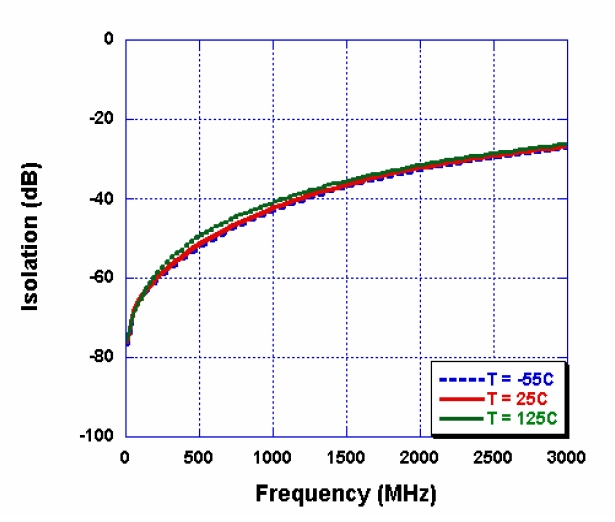
| solation – RF1 to RF2 | 2000 MHz | 24 | 28 | dB | |
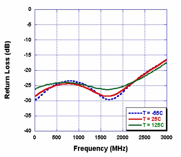
| Return Loss2 | 2000 MHz | 22 | dB | ||
| Input 1 dB Compression | 2000 MHz | 28 | 31 | dBm |
Note: 1. Device linearity will begin to degrade below 10 MHz.
Note: 2. Return loss not measured in production due to equipment
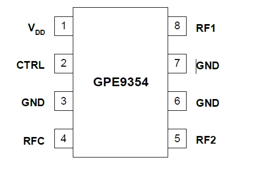
Figure 3. Pin Configuration
 | Absolute Maximum Ratings are those values listed in the above table. Exceeding these values may cause permanent device damage. Functional operation should be restricted to the limits in the DC Electrical Specifications table. Exposure to absolute maximum ratings for extended periods may affect device reliability. Electrostatic Discharge (ESD) Precautions When handling this UltraCMOS鈩?device, observe the same precautions that you would use with other ESD-sensitive devices. Although this device contains circuitry to protect it from damage due to ESD, precautions should be taken to avoid exceeding the rating specified in Table 3. Latch-Up Avoidance Unlike conventional CMOS devices, UltraCMOS鈩?devices are immune to latch-up. |
Table 2. Pin Descriptions
| Pin No. | Pin Name | Description |
| 1 | VDD | Nominal +3V supply connection. |
| 2 | CTRL | CMOS or TTL logic level: High = RFC to RF1 signal path Low = RFC to RF2 signal path |
| 3 | GND | Ground connection. Traces should be physically short and connected to ground plane for best performance. |
| 4 | RFC | Common RF port for switch.1 |
| 5 | RF2 | RF port2 .1 |
| 6 | GND | Ground Connection. Traces should be physically short and connected to ground plane for best performance. |
| 7 | GND | Ground Connection. Traces should be physically short and connected to ground plane for best performance. |
| 8 | RF1 | RF port1 .1 |
Note 1: All RF pins must be DC blocked with an external series capacitor or held at 0 VDC.
Table 3. Absolute Maximum Ratings
| Symbol | Parameter/Conditions | Min | Max | Units |
| VDD | Power supply voltage | -0.3 | 4.0 | V |
| VI | Voltage on any input except for the CTRL input | -0.3 | VDD+ 0.3 | V |
| VCTRL | Voltage on CTRL input | 5.0 | V | |
| TST | Storage temperature range | -65 | 150 | °C |
| TOP | Operating temperature range | -55 | 125 | °C |
| PIN | nput power (50 Ω) | 32 | dBm | |
| VESD | ESD voltage (Human Body Model) | 200 | V | |
| Total Dose | Total Cumulative Exposure to Ionizing Radiation | 100K | Rads(Si) |
Table 4. DC Electrical Specifications
| Parameter | Min | Typ | Max | Units |
| VDD Power Supply Voltage | 2.7 | 3.0 | 3.3 | V |
| nput Leakage | -1 | 1 | µA | |
| IDD Power Supply Current (VDD = 3V, VCNTL = 3V) | 28 | 100 | µA | |
| Control Voltage High | 0.7xVDD | 0.3xVDD | V | |
| Control Voltage Low | V |
Table 5. Control Logic Truth Table
| Control Voltage | Signal Path |
| CTRL = CMOS or TTL High | RFC to RF1 |
| CTRL = CMOS or TTL Low | RFC to RF2 |
The control logic input pin (CTRL) is typically driven by a 3-volt CMOS logic level signal, and has a threshold of 50% of VDD. For flexibility to support systems that have 5-volt control logic drivers, the control logic input has been designed to handle a 5-volt logic HIGH signal. (A minimal current will be sourced out of the VDD pin when the control logic input voltage level exceeds VDD.)
Typical Performance Data @ -55 °C to 125 °C
| Figure 4. Insertion Loss – RFC to RF1 | Figure 5. Input 1dB Compression Point |
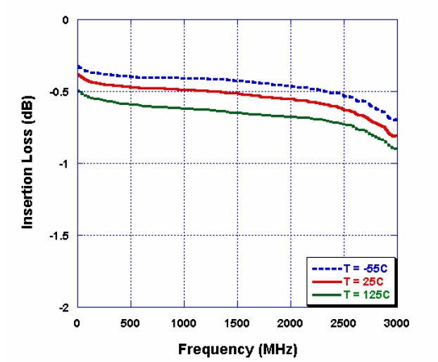 |  |
| Figure 6. Insertion Loss – RFC to RF2 | Figure 7. Isolation – RFC to RF1 |
 |  |
| Figure 8. Isolation – RFC to RF2 | Figure 9. Isolation – RF1/RF2 to RF2/RF1 |
|  |
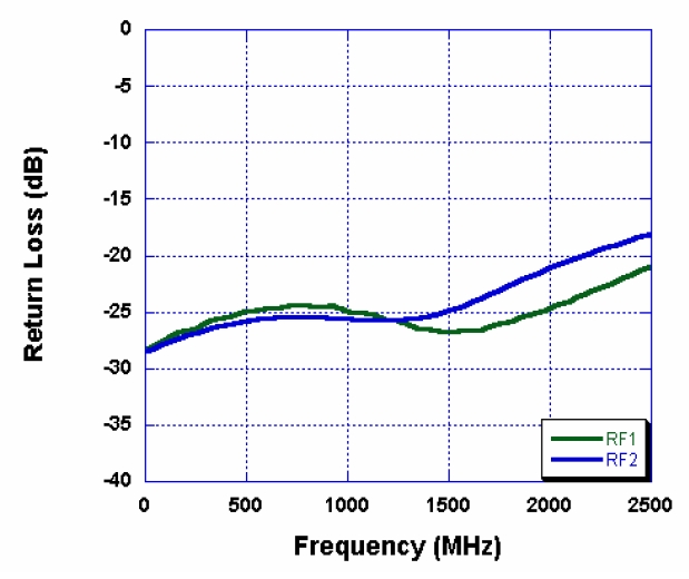
| Figure 10. Return Loss – RFC | Figure 11. Return Loss – RF1, RF2 |
 |  |
| Evaluation Kit Information Evaluation Kit | Figure 12. Evaluation Board Layouts |
| The SPDT Switch Evaluation Kit board was designed to ease customer evaluation of the PE9354 SPDT switch. The RF common port is connected through a 50 Ω transmission line to the top left SMA connector, J1. Port 1 and Port 2 are connected through 50 Ω transmission lines to the top two SMA connectors on the right side of the board, J2 and J3. A through transmission line connects SMA connectors J4 and J5. This transmission line can be used to estimate the loss of the PCB over the environmental conditions being evaluated. The board is constructed of a two metal layer FR4 material with a total thickness of 0.031”. The bottom layer provides ground for the RF transmission lines. The transmission lines were designed using a coplanar waveguide with ground plane model using a trace width of 0.030”, trace gaps of 0.007”, dielectric thickness of 0.028”, metal thickness of 0.0014” and εr of 4.4. J6 provides a means for controlling DC and digital inputs to the device. Starting from the lower left pin, the second pin to the right (J2-3) is connected to the device CNTL input. The fourth pin to the right (J2-7) is connected to the device VDD input. A decoupling capacitor (100 pF) is provided on both CTRL and VDD traces. It is the responsibility of the customer to determine proper supply decoupling for their design application. Removing these components from the evaluation board has not been shown to degrade RF performance. The ground plane has been removed from beneath the device for performance issues. It was found that insertion loss dips (suck-outs) were experienced due to the capacitive effect of the metal package sitting insulated by the solder-mask on the ground plane. All data specified and shown on this datasheet was taken using this evaluation board configuration. For optimal performance, the package may be soldered directly to the ground plane, but the reliability issues associated with this mounting must be addressed by the customer. | 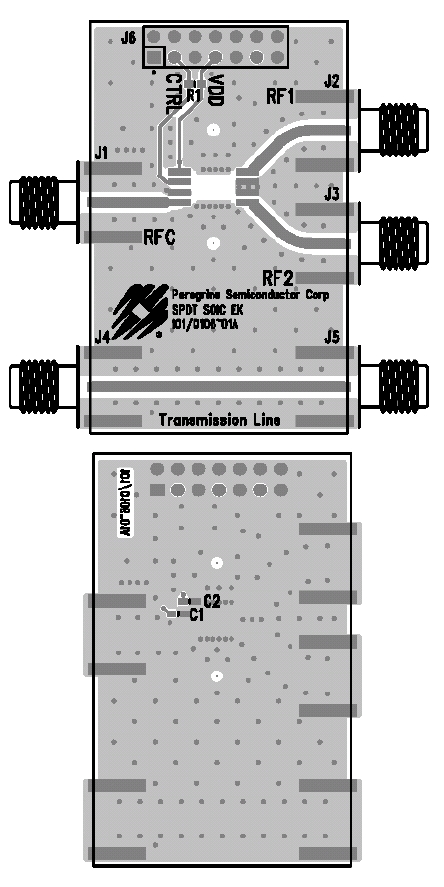 |
| Figure 13. Evaluation Board Schematic Peregrine specification 102/0129 | |
 | |
Figure 14. Package Drawing
8-lead CSOIC
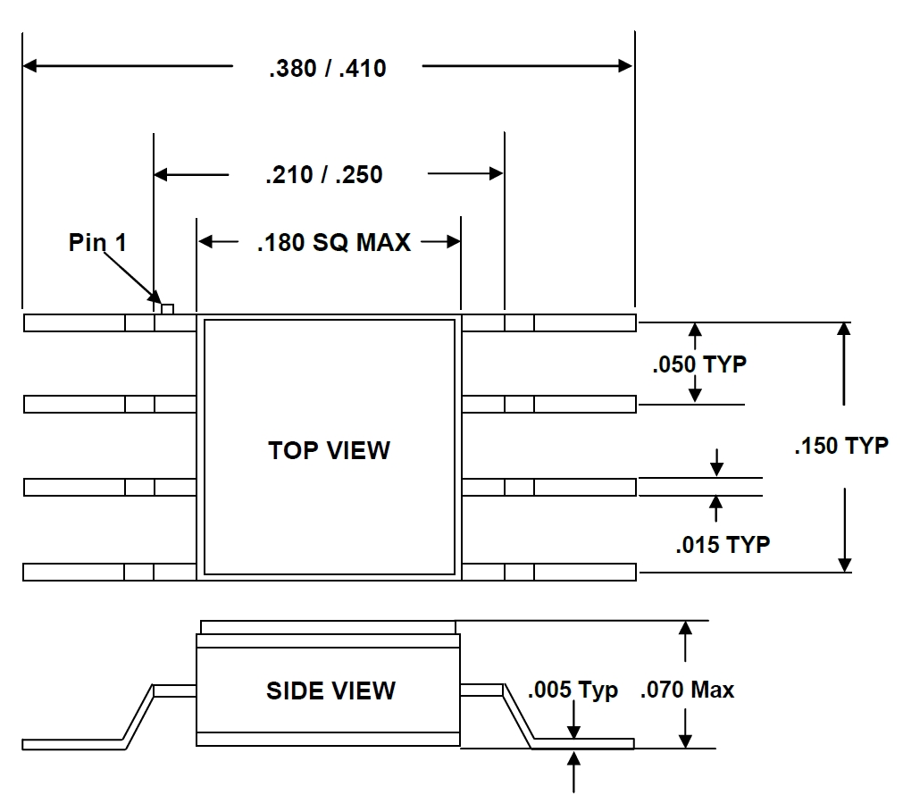
Table 6. Ordering Information
| Order Code | Part Marking | Description | Package | Shipping Method |
| 9354-01 | GPE9354 ES | Engineering Samples | 8-lead Ceramic SOIC | 50 units / Tray |
| 9354-11 | GPE9354 | Flight Units | 8-lead Ceramic SOIC | 50 units / Tray |
| 9354-00 | GPE9354-EK | PE9354 Evaluation Kit | Evaluation Kit | 1 / Box |
Previous
Next
Inquire Now
Note: Please leave your email address, our professionals will contact you as soon as possible!
Related Products