
Products
Related Posts
What is
Switch
?

We has volume-produced high-precision analog-to-digital converters (ADC), digital-to-analog converters (DAC), and clock driver chips, all
of which have achieved industry-leading specifications. Additionally, these products are capable of seamless pin-to-pin replacements with other
advanced chip products. Our ADC and DAC products are renowned for their exceptional accuracy, low power consumption, and high speed,
meeting the diverse application requirements ranging from industrial automation to communication systems, and medical devices. These
products are meticulously designed to ensure stable and reliable performance under various harsh environments. Clock driver chips represent
another core technology of ours, providing precise timing control for high-speed data transmission and being indispensable components in many
high-performance computing and communication systems. Our clock driver chips feature low jitter, high-frequency stability, and excellent phase
noise performance, ensuring system synchronicity and overall functionality. The volume-produced MCU chips are celebrated for their high
performance, low power consumption, and extensive integrated functionalities, catering to a wide range of applications from automotive, smart
home devices to industrial automation, and IoT devices. These products are carefully engineered to deliver stable and reliable performance under
stringent environmental conditions.
div[class^="e_richText"] .table table.buyao td {border:none !important;}


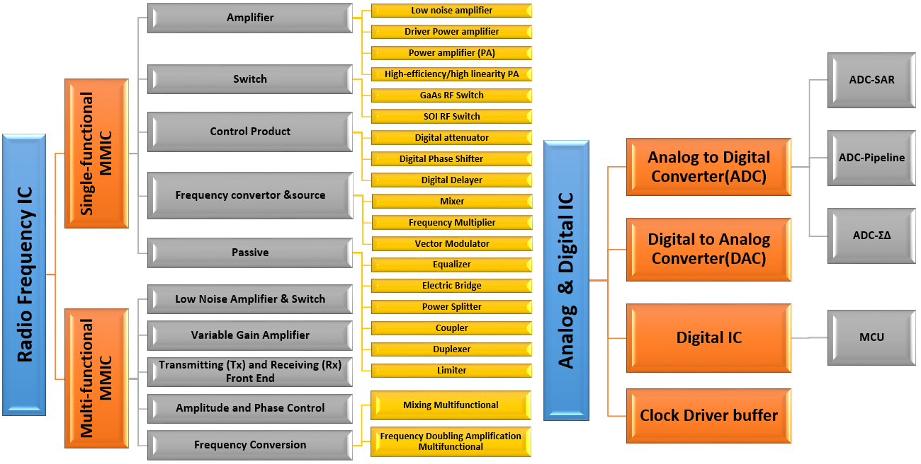
Roadmap of IC
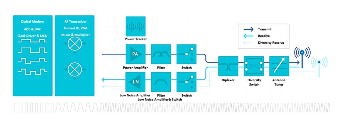
Application of ICs in the communication system
GaAs RF Switch
| Product | Type | Frequency (GHz) | Insertion loss (dB)) |
Isolation (dB) |
VSWR | switching speed(ns) | control signal(V/V) | Size (mm) |
| GAC0130 | 2×SPDT | 0.3~2 | 8.5 | 50 | 1.5 | 60 | 0/+5 | 3 × 3 QFN |
| GAC0135 | 2×SPDT | 0.3~2 | 2 | 50 | 2 | 60 | 0/+5 | 4 × 4 QFN |
| GAC0102 | SPST | 20~22.5 | 2.5 | 60 | 1.2 | 20 | 0/-5 | 4 × 4 QFN |
| GAC0113 | SPST | 0.5~50 | 0.6 | 25 | 1.2 | 20 | 10mA/-5V | 5 × 3.4 BGA |
| GAC0114 | SPST | 0.5~18 | 1.5 | 40 | 1.4 | 20 | 0/+5 | 3 × 3 QFN |
| GAC0120 | SPST | DC~40 | 0.8 | 30 | 1.4 | 20 | 0/-5 | 3 × 3 QFN |
| GAC0122 | SPST | DC~40 | 1 | 30 | 1.3 | 30 | 0/+5 | 3.7×2.6×0.1 |
| GAC0125 | SPST | DC~18 | 1.7 | 50 | 1.2 | 20 | 0/-5 | 2.3×1.4×0.1 |
| GAC0128 | SPST | DC~18 | 1.6 | 60 | 1.3 | 20 | 0/-5 | 3.1×1.63×0.1 |
| GAC0137 | SPST | 0.5~18 | 1.2 | 40 | 1.3 | 30 | 0/+5 | 1.5×1.2×0.1 |
| GAC0101 | SPDT | DC~2 | 0.6 | 36 | 1.35 | 15 | 0/-40 | 1×1.2×0.1 |
| GAC0103 | SPDT | 0.1~4 | 1.2 | 40 | 1.4 | 60 | 0/+5 | 3×3×1.1SOP |
| GAC0106 | SPDT | 25~40 | 1.8 | 32 | 1.3 | 30 | 0/+5 | 1.2×1.05×0.1 |
| GAC0107 | SPDT | 0.5~50 | 0.6 | 28 | 1.4 | 20 | 10mA/-10mA | 1.25×0.78×0.1 |
| GAC0108 | SPDT | DC~18 | 2 | 45 | 1.3 | 20 | 0/-5 | 1.5×1.5×0.1 |
| GAC0109 | SPDT | DC~7 | 0.5 | 25 | 1.3 | 500 | 3.3 | 1 × 1 QFN |
| GAC0112 | SPDT | DC~7.125 | 0.5 | 30 | 1.4 | 265 | 1.8 | 1 × 1 QFN |
| GAC0115 | SPDT | 0.5~18 | 2 | 47 | 1.4 | 20 | 0/+5 | 1.5×1.2×0.1 |
| GAC0117 | SPDT | DC~12 | 1 | 50 | 1.3 | 20 | 0/-5 | 1.5×1.5×0.1 |
| GAC0118 | SPDT | 0.1~4 | 0.5 | 43 | 1.4 | 300 | 1.8 | 4 × 4 QFN |
| GAC0119 | SPDT | 2~18 | 1.1 | 28 | 1.4 | 20 | 0/+5 | 0.82×1.8×0.1 |
| GAC0121 | SPDT | DC~7 | 1 | 55 | 1.2 | 10 | 0/-5 | 1.44×1.12×0.1 |
| GAC0124 | SPDT | DC~6 | 0.8 | 44 | 1.4 | 200 | 3.3 | 1.5 × 1.5 DFN |
| GAC0126 | SPDT | 20~22.5 | 2.2 | 50 | 1.3 | 20 | 0/-5 | 1.2×1.1×0.1 |
| GAC0132 | SPDT | 0.1~6 | 1.4 | 45 | 1.4 | 300 | 0/+5 | 4 × 4 QFN |
| GAC0133 | SPDT | DC~15 | 1.2 | 50 | 1.3 | 20 | 0/-5 | 2.05×1.04×0.1 |
| GAC0134 | SPDT | 25~40 | 2 | 36 | 1.5 | 20 | 0/-5 | 1.05×1.2×0.1 |
| GAC0136 | SPDT | DC~12 | 1.3 | 50 | 1.5 | 40 | 0/+5 | 1.6×1.0×0.1 |
| GAC0138 | SPDT | 0.1~8 | 0.75 | 55 | 1.3 | 250 | 1.8 | 4 × 4 QFN |
| GAC0140 | SPDT | DC~6 | 1 | 41 | 1.5 | 15 | 0/-40 | 0.95×1.8×0.1 |
| GAC0142 | SPDT | DC~12 | 1.3 | 50 | 1.3 | 45 | 0/+5 | 4×4QFN |
| GAC0123 | SP3T | DC~6 | 2.3 | 50 | 1.4 | 20 | 0/+5 | 1.5×2×0.1 |
| GAC0127 | SP3T | DC~18 | 1.8 | 45 | 1.3 | 20 | 0/-5 | 1.5×1.5×0.1 |
| GAC0111 | SP4T | DC~6 | 1.4 | 39 | 1.5 | 100 | 0/+5 | 4 × 4 CQFN |
| GAC0116 | SP4T | DC~10 | 1.5 | 50 | 1.4 | 30 | 0/+3.3 | 1.6×1.9×0.1 |
| GAC0131 | SP4T | DC~4 | 1.4 | 35 | 1.3 | 60 | 0/+5 | 3 × 3 QFN |
| GAC0141 | SP4T | DC~4 | 1.2 | 39 | 1.4 | 100 | 0/+5 | 1.5×1.5×0.1 |
| GAC0104 | SP5T | 0.1~50 | 1.2 | 43 | 1.4 | 20 | 10mA/-10mA | 1.62×1.54×0.1 |
| GAC0105 | SP5T | 0.4~4 | 0.6 | 55 | 1.2 | 300 | 1.8 | 4 × 4 QFN |
| GAC0139 | SP5T | 0.1~8 | 1.2 | 55 | 1.4 | 280 | 1.8 | 4 × 4 QFN |
| GAC0110 | SP8T | 0.5~50 | 0.8 | 35 | 1.5 | 20 | -15mA/0V | 2.6×1×0.1 |
| GAC0129 | SP8T | 0.5~50 | 2.2 | 40 | 2 | 20 | -15mA/0V | 2.37×1.27×0.1 |
SOI RF Switch
| Product | to Replace | Type | Frequency (GHz) | Insertion loss (dB) |
Isolation (dB) |
switching speed(ns) | control signal(V/V) | Size (mm×mm) |
| GAE0201 | PE42452 | SP5T | 0.45~4 | 0.9 | 53 | 160 | 3.6/1.8 | 4×4 QFN |
| GAE0202 | - | SPDT | DC~7.125 | 0.58 | 22 | 150 | 3.3/1.8 | 1×1 QFN |
| GAE0203 | RFSW6024 | SPDT | 0.005~6 | 0.8 | 63 | 230 | 3.3/1.8 | 4×4 QFN |
| GAE0204 | - | SPDT | 0.1-8 | 0.8 | 60 | 350 | 3.3/1.8 | 4×4 QFN |
| GAE0205 | PE42424 | SP5T | 0.4~6.5 | 1.3 | 58 | 300 | 3.6/1.8 | 4×4 QFN |
| GAE0206 | PE42420 | SPDT | 0.1~7.125 | 1.2 | 63 | 305 | 3.3/1.8 | 4×4 QFN |
Previous
Next
Inquire Now
Note: Please leave your email address, our professionals will contact you as soon as possible!
Related Products